Download
1 / 20
200 likes | 208 Views
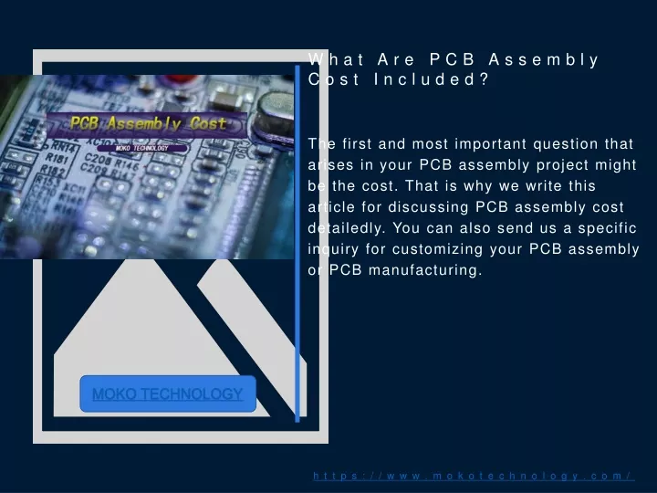
The first and most important question that arises in your PCB assembly project might be the cost. That is why we write this article for discussing PCB assembly cost detailedly. You can also send us a specific inquiry for customizing your PCB assembly or PCB manufacturing.<br>

E N D
What Are PCB Assembly Cost Included? The first and most important question that arises in your PCB assembly project might be the cost. That is why we write this article for discussing PCB assembly cost detailedly. You can also send us a specific inquiry for customizing your PCB assembly or PCB manufacturing. MOKO TECHNOLOGY https://www.mokotechnology.com/
What constitutes PCB assembly cost? 1 At this point we would like to briefly give an insight into what the prices for the assembly of electronics generally consist of. Basically, a generalization based on a price per component to be assembled is not meaningful. Such offers at low prices are often only intended to arouse customer interest and can usually only be achieved by purchasing large quantities of printed circuit board. A real calculation for your pcb assembly cost is much more individual. 3 4 https://www.mokotechnology.com/
What constitutes PCB assembly cost? For a targeted offer, not only the components to be assembled are considered, but also e.g. the number of individual circuit boards or benefits. A single circuit board with 1000 components is easier to handle than 1000 circuit boards with only one component. Furthermore, the one sided PCB or double-sided pcb assembly plays a major role. With the double sided PCB assembly, almost all work steps occur twice. For a targeted offer, not only the components to be assembled are considered, but also e.g. the number of individual circuit boards or benefits. A single circuit board with 1000 components is easier to handle than 1000 circuit boards with only one component. Furthermore, the one sided PCB or double-sided pcb assembly plays a major role. With the double sided PCB assembly, almost all work steps occur twice. An SMD stencil for paste printing must also be taken into account. In addition, there may be an additional effort for bonding heavier components to the underside. Finally, the component shapes used and the manufacturability of the assembly are taken into account. All these points are the basis for the calculation. The result is a targeted price for your assembly. https://www.mokotechnology.com/
Using the technically feasible is not always the most practical thing On PCB transmission lines, the engendering delay is given by: Everything is getting smaller and more complex. But what does the use of ever smaller components mean for quality and what effects does this have on the price for the manufacture of electronics? In general, one can say that the smaller the components, the worse they are visually, i.e. they are worse and more difficult to control. Additional test steps, such as X-raying BGAs, may be necessary. In addition, the small size places higher demands on the manufacturing technology and requires a high degree of precision in the PCB layout (footprints, template data, etc.). Even the smallest mistakes often have serious consequences and have a direct impact on the manufacturability and quality of the PCB assembly. All of this increases the PCB assembly cost for the SMD assembly! https://www.mokotechnology.com/
Using the technically feasible is not always the most practical thing On PCB transmission lines, the engendering delay is given by: When designing and developing electronics, you should therefore ask yourself whether your application requires the use of the smallest SMT sizes (e.g. 0201, pitch 0.3, etc.). If your module offers enough space, check the designs used and check alternatives. Larger PCB components save money, time and – yes – nerves when manufacturing and commissioning electronics. https://www.mokotechnology.com/
Lower costs for electronics production On PCB transmission lines, the engendering delay is given by: There are many ways to optimize the cost of manufacturing your electronics. If you can answer YES to the following points, you have already taken advantage of the simplest options: • Registration marks or fiducials are provided on the printed circuit board and in the Pick & Place data.• The Bill of Material (BOM, component list) contains all information and complete manufacturer names.• All information, such as component designation, polarities, etc., is contained in the assembly plan and is easy to read.• The designs of the individual components have been selected economically and practically sensibly (see above).• The layout specifications, explicit for the component footprint, are implemented in the PCB layout according to the manufacturer’s specifications.• The technology used for the layout was based on common manufacturer standards. https://www.mokotechnology.com/
Factors that affect the PCB assembly cost On PCB transmission lines, the engendering delay is given by: • Incomplete specifications, missing information and / or insufficient data provision for your project.• Designs such as BGAs, components smaller than 0402 or with a pitch smaller than 0.4mm must be used.• The PCB technology deviates from the standard, e.g. Blind buried vias, micro vias, fine conductors, etc.• Components that are difficult to obtain or discontinued are used. Of course, the time factor also plays a role. If your project is time-critical and runs as a rush order, the production planning for your order must be specially adapted – and quickly! https://www.mokotechnology.com/
Specification that can help calculate your PCB assembly cost On PCB transmission lines, the engendering delay is given by: The following criteria must be met in order to populate your boards according to this calculation: ♦ PCB size: min. 40x40mm max.160 x 200mm♦ Smallest component 0402- SOIC, PLCC, TSOP, QFP’s, smallest grid 0.65mm♦ Deliveries of belt sections and individual parts are clearly marked.♦ Please note that components can be lost during set-up and during assembly. Approximately 30% of small components should be delivered more. https://www.mokotechnology.com/
Specification that can help calculate your PCB assembly cost On PCB transmission lines, the engendering delay is given by: ♦ ICs etc. min. 1 piece more (depending on the type of packaging, legs may be damaged or bent)♦ We need data for the solder paste template in Ext.Gerber RS-274 or Eagle Board file. These are checked by us and modified and manufactured according to IPC-7525A.♦ Max. 1500 openings per template♦ We need a data format for the assembly program XY coordinates with direction of rotation and component assignment.♦ To check the components with your data, an Excel BOM file based on our template. (see sample in our download area) https://www.mokotechnology.com/
THT assembly compared to the SMD method On PCB transmission lines, the engendering delay is given by: In contrast to the SMD assembly, a wired component is inserted into the existing recesses with the THT assembly. This is done mechanically and does not require manual soldering. As a rule, a wave soldering system or a selective soldering system is used for the soldering. Everything have advantages and disadvantages. However, this does not change the quality of the SMD or THT assembly, and both methods are also approximately the same in terms of cost. Compared to the SMD variant, the advantage of THT assembly is that the soldered joints can still be clearly seen; with the SMD method, the soldered joints can only be identified by X-ray. THT assemblies are particularly recommended for larger assemblies, since SMD variants are more suitable for small printed circuit boards, as these otherwise have an insufficient mechanical capability. https://www.mokotechnology.com/
SMD manufacturing at low cost On PCB transmission lines, the engendering delay is given by: The assembly of printed circuit boards in SMD production can be carried out at extremely low costs. Since little space is required, there is hardly any material, because SMD production involves soldering in a very small space. In SMD production, this not only works very quickly, but also very inexpensively, not only because it can be loaded on both sides. The soldering is no longer recognizable, but it is precisely for this reason that the SMD manufacturing method is so efficient. The weight of the circuit board is very low, which makes it more susceptible to mechanical influences, the connecting wires are omitted and the circuit board material can be made even thinner. https://www.mokotechnology.com/
SMD manufacturing at low cost On PCB transmission lines, the engendering delay is given by: The small-scale nature of SMD production only permits labeling using a code. Manual soldering is not possible in SMD production and manual improvements are also difficult to carry out. However, due to the small size, it is not very economical to manually rework components in SMD production, since replacing the components is usually faster, cheaper and easier. https://www.mokotechnology.com/
PCB boards fixing for decreasing PCB assembly cost On PCB transmission lines, the engendering delay is given by: With quantities of 20-50 pieces or more, the assembly of printed circuit boards usually has economic advantages: For some of the operations in the assembly of printed circuit boards, it does not matter whether you process a single circuit board or several boards in use. For example, a 10-fold benefit in board assembly causes the same costs of a single board in certain work steps and thus only a tenth of the cost per board. https://www.mokotechnology.com/
PCB boards fixing for decreasing PCB assembly cost On PCB transmission lines, the engendering delay is given by: In the case of rectangular boards, the design of the panels is preferably in the scratch panel. In the case of non-rectangular boards, a combination of scratches and milling is often used to achieve economical board assembly. If this is not possible, the milling benefit remains, in which the boards are connected to one another by webs. However, these benefits are somewhat less stable and therefore have certain disadvantages when it comes to PCB assembly. The benefits are usually separated with a separator before delivery. Scratches can be separated very cleanly, but bar sills often require reworking for clean edges. https://www.mokotechnology.com/
PCB boards fixing for decreasing PCB assembly cost On PCB transmission lines, the engendering delay is given by: Benefit optimization is one of the most important cost considerations, especially for SMD assembly. We advise you individually, you are welcome to contact us before the layout is finished. Sometimes we can still take into account information that makes the boards easier, safer or cheaper to produce or equip. If you leave the procurement of the blanks to us, we will of course take care of the optimal benefits. https://www.mokotechnology.com/
PCB boards fixing for decreasing PCB assembly cost On PCB transmission lines, the engendering delay is given by: The circuit board can be assembled on one or both sides. Often, one-sided assembly is cheaper at first. However, if one looks at the cost of the end product, a smaller board could lead to a downsizing of the housing, of the entire product. And depending on the circumstances, the costs saved in the case of one-sided circuit board assembly are ultimately negligible in relation to the additional costs of a significantly larger end product. After all, double-sided SMD assembly with modern soldering systems is no longer rocket science. https://www.mokotechnology.com/
PCB assembly – highest performance for attractive costs On PCB transmission lines, the engendering delay is given by: In addition to the production of printed circuit boards, PCB assembly is the key process, because this is the only way to create electrical connections on a printed circuit board, which are then used in a wide variety of electronic devices. If you would like to order a PCB, you should not only manufacture it, but also have it assembled so that it becomes functional. Are you looking for a PCB assembly specialist? Then look no further, because with Intec TIV you are in the right place. We have been manufacturing and assembling printed circuit boards since our foundation more than 40 years ago and have been part of the largest printed circuit board manufacturer in Slovenia for some time. Because more and more foreign customers want us to manufacture and assemble a PCB, we also offer our expertise in Germany and Austria. So you can now secure our PCB service in Berlin and other cities if you are looking for high-quality PCB assembly and prototype production, whether for 4 layers or more. https://www.mokotechnology.com/
Have PCB manufactured in China On PCB transmission lines, the engendering delay is given by: Since the customer requirements are very different, we use different drilling machines, which enable a cost-efficient and smooth PCB assembly. The tolerance of drilling is +/- 0.05 mm and the maximum working format is 750 mm x 650 mm. If you choose to use THT technology, the drilling diameter can range from 0.1 mm to a maximum of 6.4 mm. https://www.mokotechnology.com/
Innovative processes for best results On PCB transmission lines, the engendering delay is given by: An important process step before PCB assembly is the pressing of printed circuit boards. If you have your PCB manufactured by us, it will be pressed with a 2 or 3-tier vacuum press, combined with a DIS PRS-77 L / U binding system, which guarantees optimal results. The maximum working format is 650 mm x 550 mm, and it is also possible to join two intermediate layers by welding. The minimum thickness of an intermediate layer is 0.05 mm. In order for the PCB assembly or prototype production to be carried out optimally, each individual board must meet the highest quality standards. That is why every process step is closely monitored and documented. We use the Orbotech Fusion 22 control machine to control the intermediate and outer layers during the manufacturing process. This is the only way to ensure consistently high quality, be it in the PCB manufacture or PCB assembly. That is why it is particularly worthwhile to have a PCB manufactured in our company, not to mention attractive costs. https://www.mokotechnology.com/
Extensive assortment – circuit board manufactured in China We have been following the trends in PCB assembly and prototype production for more than 40 years and know that the demands on manufacturers are increasing. In order to do justice to this, we work closely with ProPlace, the leading Slovenian expert for PCB assembly. By having prototypes or a PCB manufactured by us, you get a complete product, not just a customized printed circuit board, but you can also equip it with electrical components MOKO TECHNOLOGY