Download
1 / 20
200 likes | 202 Views
With the use of a rigid flex PCB(rigid FPC), flexible circuit substrates and rigid circuit substrates are covered together. Rigid-flex PCBs cross the limits of conventional rigid PCBs and the one of a kind properties of flex circuits that utilization high-flexibility electrodeposited or moved strengthened copper conductors photograph carved onto a flexible protecting film.<br>Flex circuits incorporate stack-ups produced using a flexible polyimide, for example, Kapton or Norton and copper-covered together through warmth, acrylic cement, and weight.<br><br>

E N D
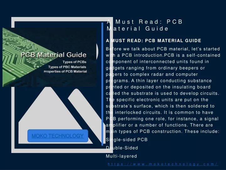
A Must Read: PCB Material Guide A MUST READ: PCB MATERIAL GUIDE Before we talk about PCB material, let’s started with a PCB introduction.PCB is a self-contained component of interconnected units found in gadgets ranging from ordinary beepers or pagers to complex radar and computer programs. A thin layer conducting substance printed or deposited on the insulating board called the substrate is used to develop circuits. The specific electronic units are put on the substrate’s surface, which is then soldered to the interlocked circuits. It is common to have PCB performing one role, for instance, a signal amplifier or a number of functions. There are main types of PCB construction. These include: Single-sided PCB Double-Sided Multi-layered MOKO TECHNOLOGY https://www.mokotechnology.com/
A MUST READ: PCB MATERIAL GUIDE 1 PCB is the most critical part component of electronics. You may have heard of the printed writing cards or printed writing board when individuals talk about PCB. Well, there is no difference between these terms; they mean the same thing. Due to their significance in all electronics, including computers and calculators, the board material for the PC is chosen with a lot of care and caution. The person making the selection must have knowledge of the electrical requirements of any type of equipment. 3 https://www.mokotechnology.com/ 4
A MUST READ: PCB MATERIAL GUIDE Prior to the establishment of PCB, the materials used for early boards were often covered by shells of knotted overlapping wirers, which could fail at particular junctures. When used for relatively long, they could as well short circuit, and some wires could start cracking. Expectedly, the manual process used in making these boards was so demanding, confusing, and meticulous. Since many electronics started depending on circuit boards, it became increasingly necessary to come up with modest, more compact options, and this is precisely what led to the emergence of PCB material. Importantly, the metal, which enhances the flow of current between the board and the components attached, is referred to as solder. This substance has dual roles considering its adhesive features. This blog covers all the details you need to know about PCB materials. So read to the end, and you will enrich your knowledge and perhaps make the right choice when required. https://www.mokotechnology.com/
The Basic Properties of PCB Material This is perhaps the most crucial aspect you need to pay attention to. As we mentioned at the outset, you need to be careful while selecting the PCB material, and being acquainted with the properties is so crucial. In this section, we are going to look at thermal, electrical, and chemical properties. So let us begin Thermal Properties As the title suggests here, we examiner the effect of temperature. Pay attention to the following. The Glass Transition temperature. Temperature ranges affect PCB material significantly. Generally, the substrate softens if subjected to a temperature beyond the required threshold. But again, the substrate will harden when taken back or when the temperature is readjusted to normal. The range where transformation can possibly occur is called glass transition temperature (Tg). This unit is determined in degrees celsius. https://www.mokotechnology.com/
The Basic Properties of PCB Material The Decomposition temperature. This is a temperature within which decomposition of the PCB material takes place. Generally, when the substrate is in temperature beyond a particular threshold, it decomposes. Unlike in glass transformation, the effects of substrate decomposition are irreversible. Why does this imply? People work in different environments with different temperature ranges. When selecting a PCB substrate, you need to ensure it is really compatible with your working environment. https://www.mokotechnology.com/
The Basic Properties of PCB Material Coefficient of Thermal Expansion. The expansion rate of any PCB substrate is the CTE. Whenever a material his subjected to a temperature beyond its Tg, the CTE rises, and this is quantified in parts per million (ppm). A PCB material often has a greater CTE compared to a copper layer. In most cases, this deviation in temperature is the leading problem of interconnection issues when heated. However, because of the constraints in the PCB material as a result of the glass woven, CTE is generally within 10 to 20 ppm in the X and Y axes. In case the temperature goes beyond the Tg limit, the CTE does not change. https://www.mokotechnology.com/
The Basic Properties of PCB Material Thermal conductivity. The heat conductive characteristics of PCB material is called thermal conductivity (k). The thermal conductivity of a substance is directly related to the potential of a PCB material to transfer heat. The thermal conductivity is determined in in watts per meter (w/m), expressed in kelvin (k) In light of the above, the thermal properties of a PCB substrate is a vital factor for consideration. PCB materials are significantly affected by temperature ranges, and so you should pay attention to the conditions in your working environment. What about the electrical properties? https://www.mokotechnology.com/
The Basic Properties of PCB Material Electrical Properties of PCB material There are several electrical characteristics you need to consider when it comes to the choice of a PCB material. The following is a brief overview of some of them. Dielectric constant. This feature is Relative Permittivity. Impedance and integrity are the two most significant factors for consideration when it comes to the electrical performance of a PCB substrate. The dielectric constant of a PCB material range from 3.3 to 5.5. This value is affected by frequency. Specifically, it is inversely related to the frequencies. Nevertheless, Er changes differently in different materials. It changes less in others and more in others. For a substrate to be safer for use in high-frequency applications, it should have a stable dielectric constant in wide frequency ranges. https://www.mokotechnology.com/
The Basic Properties of PCB Material Dielectric Loss Tangent (Tan δ). It is also the Dissipation Factor (Df). If a material has a low loss tangent, it actually loses less power. The loss tangent applied in the PCB materials often varies from 0.02 to o.oo1. The higher value applies to most of the materials, while the latter one is used in the high-end materials. Besides, the loss tangent is also affected by the frequencies. It increases with a rise in frequencies. However, on the basis of digital circuitry, the loss tangent is not very significant. https://www.mokotechnology.com/
The Basic Properties of PCB Material Volume Resistivity (ρ). This is the resistance of any dielectric substance to insulation or perhaps electricity. If a PCB substrate has a great resistivity, it is not likely to expedite electric charges. The resistivity of any dielectric substance is measured in ohm-meters (Ω-m) or ohm-centimeters (Ω-cm). Just like in the dielectric insulators, all the materials on the PCB needs to have high resistivity. The preferred resistivity value range between 103 and 1010 Megaohm-centimeters. Nevertheless, external factors such as significant temperature variations and humidity influence the resistivity of a substance. Surface Resistivity (ρS). This is the surface resistance of a dielectric substance to insulation as well as electricity. Just like the volume resistivity of a material, surface resistivity needs to be high. It should range between 103 and 109 megaohms per square. Also, differences in temperature and moisture influence surface resistivity. https://www.mokotechnology.com/
The Basic Properties of PCB Material Electrical Strength. Throughout the Z direction of a PCB substrate, the potential of a dielectric substance to withstand electrical breakthrough is called electrical strength. This is determined in volts/mil. Most PCB substrate’s electrical strength falls between 800 V/mil and 1500 V/mil. Indisputably, the electrical characteristics of a PCB material is a vital factor for consideration. From the above discussion, it is crucial to pay attention to these properties when making your choices. Let us now look at other aspects of PCB material properties. https://www.mokotechnology.com/
The Basic Properties of PCB Material Chemical Properties The following are the critical properties for consideration in this regard. Flammability Specs (UL94) Moisture Absorption. This is the capacity of a dielectric substance to resist exposure to a liquid. The moisture absorption figure for many PCB materials ranges from 0.01% to 0.2%. In general, moisture absorption affects both the electrical and thermal characteristics of dielectrics. Methylene Chloride Resistance (MCR). This is the chemical resistance of any PCB substance. This measures the dielectric strength of methylene chloride absorption. The MCR often ranges from 0.01% to 0.20%. https://www.mokotechnology.com/
The Basic Properties of PCB Material Types of PCBs As we stated at the outset, there are three main variants of PCB materials. Let us now review them in detail. Single-layer PCBs As the name suggests, this is a PCB made from one layer of the base substance. Usually, a tinny metal layer covers one side of the base substrate. Since copper is the most fantastic electrical conductor, it is always preferred as a coating. Upon applying the copper base platting, a protective solder mask is often applied. Finally, the last silk-screen is used to mark out all the essential units on the board. Single-layer PCBs are quite easy to create and manufacture. This is due to the fact that they have different circuits and units soldered on a single side. For this reason, single layer PCBs can be acquired at relatively lower prices, especially where one makes a large volume purchase. They are used for different applications such as calculators, printers, and power supplies, among others. https://www.mokotechnology.com/
The Basic Properties of PCB Material Double layer PBCs Unlike single-layer PBCs, double layer PBCs are characterized by base material having a slim layer of a conductor, such as copper on both sides. Holes are often drilled on the board to enable circuits on one section of the board to link to the circuits on the end. In the double layer PCB board, the circuit and the components are often linked in two ways. The first one can be using a through-hole and a second one utilizing a surface-mount. In general, a through-hole connection simply means the minor wires, also referred to as leads are always fed via the holes. Afterward, the leads are soldered to the appropriate component. https://www.mokotechnology.com/
The Basic Properties of PCB Material In contrast, the wires are not used in the surface mount as connectors. In this case, a lot of soldered small leads are directly linked to the board. This implies that the board itself is a wiring surface for various components. This permits the completion of the circuit with limited space. A lot of space is freed, and as a result, the board can carry out more functions at a faster speed and a lightweight compared to when through-board holes are used. Usually, double layer PCBs are utilized in the applications demanding an intermediate degree of circuit complexity, including the following: Industrial controls Power supplies Instrumentations LED lighting Automotive dashboards Amplifiers Vending machines https://www.mokotechnology.com/
The Basic Properties of PCB Material Multilayer PCBs Multilayer PBC is made up of a series of either triple or a number of double-layered PBCs. A specialized glue is often used to secure these layers before they are sandwiched between insulation units to make sure too much heat cannot melt or soften any of the individual components. Additionally, these PBCs are always in a variety of sizes. They can contain only four layers, or as many as ten or twelve. The biggest multilayer PBC ever to be designed was 50 layers in thickness. If a PBC has a lot of layers, developers can come up with quite thick, complex structure appropriate for a wide range of intricate electrical functions. Multi-layer PBCs can be pivotal in the following applications: https://www.mokotechnology.com/
The Common types of PCB Materials There are three common materials crucial in the fabrication of the PBCs. The following is a brief overview of each of the three. FR-4 This is the widely used material in the manufacture of PBCs. It is just a glass strengthened epoxy laminate sheet. The laminate that is utilized here flame retardant and also resistant to water. It also offers better strength when it comes to weight ratios. The material provides a very high tensile strength. PTFE (Teflon) This is basically a plastic substance with no resistance. For this reason, it is utilized for fast speed and frequency applications. This material has a lot of advantages. For instance, it is very flexible, making it priceless in applications having tight tolerances. Additionally, it is very lightweight, making it usable across different industries. Moreover, it is flame resistant, has great physical strength, temperature stability, and quite versatile in application. https://www.mokotechnology.com/
The Common types of PCB Materials Metal This is a conventional material of copper and aluminum, among others utilized in PCBs. They permit the usage of Surface Mount Technology for the incorporation of components. They also have mechanical durability and, therefore, can be used for long. https://www.mokotechnology.com/
The Common types of PCB Materials The Future of PCB Material The shrinking of the electronic devices will lead to the production of smaller and densely packed PCBs. These products will have significant electric potential. The development beyond the boards we just discussed here comprises of 3-dimensional molded plastic boards as well as the increased utilization of the integrated circuit chips. For this reason, the manufacture of PCBs is likely to be more dynamic in the years to come. https://www.mokotechnology.com/
The Bottom Line PCB materials have a lot of characteristics. It is essential to consider all these characteristics are essential, and you have to consider them when selecting the materials for use in this regard. Some characteristics, such as decomposition temperature and glass transition temperature, are significantly affected by temperature variations. For this reason, you are supposed to consider the temperature of your working environment when selecting PCB materials. If you need help in choosing PCB material, try seeking help from Moko Technology. MOKO TECHNOLOGY