Download
1 / 11
110 likes | 236 Views
Micro controller hardware architechture. Scope. Hardware Diagram Operating Mode Architecture installing clock external memory attachment. Pin configuration. MCS51Core CPU Atmel 89S8252. Pins. Address/Port: High address/P2: 8 pins A8-A15 or Port 2

E N D
Micro controller hardware architechture CIT 673 Created by Suriyong
Scope • Hardware Diagram • Operating Mode • Architecture • installing clock • external memory attachment CIT 673 Created by Suriyong
Pin configuration MCS51Core CPU Atmel 89S8252 CIT 673 Created by Suriyong
Pins • Address/Port: High address/P2: 8 pins • A8-A15 or Port 2 • Address/Data/Port: Low address/Data/P0 • 8 pins • A0-A7/D0-D7/Port 0 • Port: port 1 8 bits • Signal pin • ALE: Address Latch Enable : • active high, signal to express that the signal is low address at P0 • PSEN: Program Strobe Enable: • active low, signal when access to external program memory • EA: External Access: • active low, signal to control the CPU to access the external memory • RST: CPU Reset input • Signal/Alternate function port pin : port 3 • WR: Write signal to external data • RD: Read signal to external data • TXD: Transmit Data, serial communication • RXD: Receive Data, serial communication • External interrupt source and signal • Clock : pin X1 and X2 • Power Supply : VCC:GND CIT 673 Created by Suriyong
Operating Mode • 1 chip mode • operating use only CPU and its SFR • Multi-chip mode • when extend or need more peripherals • such as extend external RAM, more I/O CIT 673 Created by Suriyong
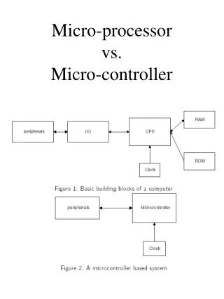
Architecture • busses • address bus • data bus • ports • registers • register that control CPU operating • clock signals • hardware connection • Address space • memory address decoding • External Input/output • address decoding and interfacing • Interrupt Hardware architechture CIT 673 Created by Suriyong
BUS • Address BUS • 16 bit able to decode of 65536 address • Use alternate function of P2 as high address bus • P0 as low address bus and multiplex with data bus • use Address Latch Enable (ALE) signal as multiplex signal • need Latching IC : 74LS373 to latch the low address • Data bus • 8 bit • alternate function of P0 • multiplex with low address bus • first as address, next as data CIT 673 Created by Suriyong
External data and program memory accessing • when external memory is needed use Program Strobe ENable (PSEN) to signal to decode the memory • when PSEN • low: program memory is accessed and data is get after Read (RD) signal is active • high: data memory is accessed and data is get or write after RD or WR signal CIT 673 Created by Suriyong
External memory diagram CIT 673 Created by Suriyong
CPU Register • Unable to manipulate directly • PC: Program Counter • Contain the address of the code • ALU: Arithmetic Logical Unit • the calculation zone CIT 673 Created by Suriyong