Download
1 / 20
220 likes | 461 Views
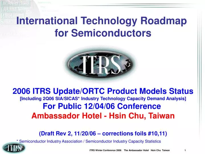
International Technology Roadmap for Semiconductors 2006 ITRS Update/ORTC Product Models Status [Including 2Q06 SIA/SICAS* Industry Technology Capacity Demand Analysis] For Public 12/04/06 Conference Ambassador Hotel - Hsin Chu, Taiwan (Draft Rev 2, 11/20/06 – corrections foils #10,11).

E N D
International Technology Roadmap for Semiconductors 2006 ITRS Update/ORTC Product Models Status [Including 2Q06 SIA/SICAS* Industry Technology Capacity Demand Analysis] For Public 12/04/06 Conference Ambassador Hotel - Hsin Chu, Taiwan (Draft Rev 2, 11/20/06 – corrections foils #10,11) * Semiconductor Industry Association / Semiconductor Industry Capacity Statistics
2005 ITRS Executive Summary Fig 5 Traditional ORTC Models Source: 2005 ITRS Document online at: http://www.itrs.net/Links/2005ITRS/Home2005.htm
ORTC Overview – 2006 Update ITRS - Unchanged *Note: Cycle = time to 0.5x linear scaling every two cycle periods ~ 0.71x/ cycle • One standard TWG table technology trend header • 2006 ITRS Update tables continue to use DRAM stagger-contacted M1 as typical industry lithography driver • Transitioned to product-oriented technology trend drivers and cycles* • ORTC Table 1a,b - MPU/ASIC M1 Half-Pitch Trend • Stagger-contacted, same as DRAM • 2.5-year Technology Cycle* (.5x/5yrs) • 180nm/2000; 90nm/2005; 45nm/2010(equal DRAM) • Then continue on a 3-year Technology Cycle*, equal to DRAM 2010-2020 • ORTC Table 1a,b - STRJ Flash Poly (Un-contacted dense lines) • 2-year Technology Cycle* (0.5x/4yrs) • 180nm/2000; 130nm/2002; 90nm/2004; 65nm/2006 • Then 3-year Technology Cycle* 1 year ahead of DRAM ’06-’20 • ORTC Table 1a,b – MPU/ASIC Printed Gate Length per FEP and Litho TWG ratio relationship to Final Physical Gate Length - 2005 ITRS targets (3-year cycle* after 2005) • TWG table Product-specific technology trend driver header items are added to individual TWG tables from ORTC Table 1a&b • Chip Size Models are connected to proposals and historical trends, incl. new Flash Model • Function Size [Logic Gate; SRAM Cell; Dram Cell; Flash Cell (SLC, MLC)] • Functions/Chip [Flash; DRAM; High Performance (hp) MPU; Cost Perf. (cp) MPU] • Chip Size [hp MPU; cp MPU; DRAM; Flash]
2005 Definition of the Half Pitch - unchanged [No single-product “node” designation; DRAM half-pitch still litho driver; however, other product technology trends may be drivers on individual TWG tables] FLASH Poly Silicon ½ Pitch = Flash Poly Pitch/2 DRAM ½ Pitch = DRAM Metal Pitch/2 MPU/ASIC M1 ½ Pitch = MPU/ASIC M1 Pitch/2 • Poly • Pitch • Metal • Pitch 8-16 Lines Typical flash Un-contacted Poly Typical DRAM/MPU/ASIC Metal Bit Line
Unchanged Fig 3 Production Ramp-up Model and Technology Cycle Timing 100M 200K Development Production 10M 20K 1M 2K Alpha Tool Beta Tool Production Tool Volume (Parts/Month) 100K Volume (Wafers/Month) 200 First Two Companies Reaching Production 10K 20 First Conf. Papers 1K 2 0 12 24 -24 -12 Months Source: 2005 ITRS - Exec. Summary Fig 3
2006 (’05-’20) ITRS Technology Trends DRAM M1 Half-Pitch : 3-year cycle All unchanged 2007 2001 2001 2003 2003 2005 2005 2006 2008 2009 2012 2015 2018 2020 14 2000 [Actual] 2000 [Actual] 2002 [Actual] 2002 [Actual] 2004 2004 2010 2013 2016 2019 65 90 90 45 32 22 16 130 130 180 180 151 107 80 71 57 50 2-Year Technology Cycle [‘98-’04] Year of Production Year of Production Year of Production 2005 ITRS Flash Poly Half-Pitch Technology: 2.0-year cycle until 1yr ahead of DRAM @65nm/’06 3-Year Technology Cycle 3-Year Technology Cycle 2008 2010 2013 2016 2019 2020 2006 2009 2012 2015 2018 Technology - Uncontacted Poly H-P (nm) Technology - Contacted M1 H-P (nm) Technology - Contacted M1 H-P (nm) 13 2001 2002 2003 2004 2006 2007 2008 2009 2012 2015 2018 2020 65 45 32 22 16 57 151 107 76 50 2010 2013 2016 2019 45 32 22 16 180 [130] 90 [ 65] 157 136 119 103 78 68 59 52 3-2-Yr Cycle] 2-Year Technology Cycle [’98-’06 ] 2.5-Year Technology Cycle 3-Year Technology Cycle 2005 ITRS MPU M1 Half-Pitch Technology: 2.5-year cycle; then equal DRAM @45nm/2010 2000 [July’02] 2005 [July’08] 14
Figure 8 ITRS Product Technology Trends - unchanged Fig 7&8 Simplified – Option 1 After 1998 .71X/2YR MPU M1 .71X/2.5YR Before 1998 .71X/3YR MPU & DRAM M1 & Flash Poly .71X/3YR Flash Poly .71X/2YR Gate Length .71X/3YR GLpr IS = 1.6818 x GLph Nanotechnology (<100nm) Era Begins -1999 2005 - 2020 ITRS Range
Fig 4 2005 ITRS Technology Cycle Timing Compared to Actual Wafer Production TechnologyCapacity Distribution ITRS Technology Cycle 10 W.P.C.= Total Worldwide Wafer Production Capacity(Relative Value *) Source: SICAS** W.P.C W.P.C W.P.C W.P.C W.P.C W.P.C W.P.C W.P.C W.P.C >0.7mm 720nm SIA/SICAS Data**: 1-yr delay from ITRS Cycle Timing to 25% of MOS IC Capacity 0.7-0.4mm 510nm 1 Feature Size (Half Pitch) (mm) 0.4-0.3mm 360nm (Feature Size of Reported Technology Capacity of SICAS Participants) <0.4mm <0.4mm <0.3mm <0.3mm 0.3- 0.2mm <0.2mm <0.2mm 255nm <0.16mm <0.16mm 0.1 <0.12mm 0.2- 0.16mm 180nm = 2003/04 ITRS DRAM Contacted M1 Half-Pitch Actual = 2005 ITRS DRAM Contacted M1 Half-Pitch Target 0.16-.12mm 127nm 3-Year Cycle 2-Year Cycle 3-Year Cycle 0.01 1997 1998 1999 2000 2001 2002 2003 2004 2005 2006 2007 <0.12mm 90nm Source: 2005 ITRS - Exec. Summary Fig 4 Year * Note: The wafer production capacity data are plotted from the SICAS* 4Q data for each year, except 2Q data for 2005. The area of each of the production capacity bars corresponds to the relative share of the Total MOS IC production start silicon area for that range of the feature size (y-axis). Data is based upon capacity if fully utilized. ** Source: The data for the graphical analysis were supplied by the Semiconductor Industry Association (SIA) from their Semiconductor Industry Capacity Statistics (SICAS). The SICAS data is collected from worldwide semiconductor manufacturers (estimated >90% of Total MOS Capacity) and published by the Semiconductor Industry Association (SIA), as of July, 2005. The detailed data are available to the public online at the SIA website, http://www.sia-online.org/pre_stat.cfm .
0.71x 0.85 to 0.72u to.60u SICAS 90nm Capacity Tracking Kickoff – 2Q06 Update 0.60 to 0.51u to.42u 0.42 to 0.36u to.30u 0.30 to 0.25u to.21u n-2 0.21 to 0.18u to.15u n-1 0.15 to 0.13u to.11u n 0.11 to 0.090u to 0.075u Next TBD?: 20% 1Q07? (2yr Cycle) 1Q08? 3yr Cycle <0.075 to 0.065u to.053u ~32% of Total MOS n+1 [available 2Q07] Technology Demand 2-year Cycle Continues! 2-yrs to >20% of Total MOS for 0.71x Technology Reduction Cycle Source: SIA/SICAS Report: www.sia-online.org/pre_statistics.cfm
SICAS 300m Capacity Tracking – 2Q06 Update 1Q97-1Q06 Total MOS 9.1% CAGR [Total MOS only – 8” Equivalent] 12.0% YoY Wafer Starts per Week (1K) 2004 – Happy 10th Anniv. SICAS! 17.4% Equiv. YoY (3 Qtrs) 1Q97-1Q06 200mm 15.3% CAGR 11.6% CAGR 12.8% YoY 43.0% Equiv. YoY (3 Qtrs) 30.8% YoY 821.4 [100%] 93.1% YoY 728.2 [100%] 362.7 [44%] 277.4 [38%] 1Q 07 1Q 97 4Q 97 4Q 07 1997 1997 2003 2004 2005 2005 2006 2006 2007 2Q06: 300mm = 25% of Total MOS 200mm = 62% of Total MOS <200mm = 14% of Total MOS 11 years intro-intro Wafer Generation 200mm/1Q97 SICAS Tracking Begins (7yrs after Intro) 300mm/1Q04 (3yrs after Intro) Source: SIA/SICAS Report: www.sia-online.org
Figure 9 ITRS Product Function Size - unchanged Fig xx Simplified Logic Gate: NO Design Area Factor Improvement (Only Scaling) SRAM: Gradual Design Area Factor Improvement DRAM: 6f2 Last Design Area Factor Improvement (@ 2 MLC bits/physical cell area) Flash: 4f2 Last Design Physical Area Factor Improvement Flash: (MLC @ 2 bits/cell = 2f2 Equivalent Area Factor) Note for Flash: SLC = Single-Level-Cell Size MLC = Multi-Level-Cell (Electrical Equivalent) Cell Size 2005 - 2020 ITRS Range
Chip Size Trends – 2005 ITRS Functions/Chip Model - unchanged (@Volume Production, Affordable Chip Size**) ** Affordable Production Chip Size Targets: DRAM, Flash < 145mm2 hp MPU < 310mm2 cp MPU < 140mm2 Average Industry 1970-2020 “Moore’s Law” 2x Functions/chip Per 2 years MPU ahead or = “Moore’s Law” 2x Xstors/chip Per 2 years Thru 2010 ** Example Chip Size Targets: 1.1Gt P07h MPU @ intro in 2004/620mm2 @ prod in 2007/310mm2 ** Example Chip Size Targets: 0.39Gt P07c MPU @ intro in 2004/280mm2 @ prod in 2007/140mm2 2005 - 2020 ITRS Range Past Future
Figure 10 ITRS Product Functions per Chip -unchanged Average Industry 1970-2020 “Moore’s Law” 2x Functions/chip Per 2 years 2005 - 2020 ITRS Range
Chip Size Trends – 2005 ITRS DRAM Model – unchanged 2005: Past Future 2005 - 2020 ITRS Range
Chip Size Trends – 2005 ITRS Flash Model - unchanged 2005: 2005 - 2020 ITRS Range Past Future
Chip Size Trends – 2005 ITRS MPU Model - unchanged Max Litho Field 2005 ITRS 834mm2 (26x32) (4x): p16h p19h p22h p10h p13h 800 26% / 2yrs 2.2Bt 4.4Bt Chip Size hp MPU = 82% SRAM Transistors, 18% Core Logic Transistors Growth 417m2 (26x16) 700 cp MPU = 58% SRAM Transistors, 42% Core Logic Transistors 2 Chips per Max Litho Field p07h p02h p04h SRAM Cell Efficiency= 60% Logic Gate Efficiency = 50% 600 1.1Bt 276Mt 552Mt MPU hp Production Chip Size 2005 ITRS (4x): MPU cp Production Chip Size 500 MPU hp Introduction Chip Size MPU cp Introduction Chip Size 400 p16c p19c p22c p10c p13c 3.1 768Mt 1.5Bt (mm2) p10h p07h p04h p98h p00h p02h 2.2Bt Affordable hp MPU 1.1Bt 552Mt 69Mt 138Mt 276Mt 300 310mm2 prod Target: 8G p07c p00c p02c p04c 384Mt 48Mt 96Mt 192Mt 200 p07c p10c p13c p00c p02c p04c Affordable cp MPU 384Mt 768Mt 1.5Bt 48Mt 96Mt 96Mt 140mm2 prod Target: 100 DRAM 0 HP 1995 1998 2001 2004 2007 2010 2013 2016 2019 2022 2025 WAS/IS: 64 45 32 16 90 22 11 8 180 128 360 255 8 MPU: 90 68 45 32 22 16 11 180 136 360 255 [2.5yr Technology Cycle Year of Introduction and Production 2000-2010] 2005 - 2020 ITRS Range Past Future
Summary – 2006 Update • DRAM Model stagger-contacted M1 unchanged from 2005 ITRS (3-year cycle* after 2004). • MPU M1 stagger-contact half-pitch unchanged on a 2.5-year cycle* through 2010/45nm, then 3-year cycle*. • Flash Model un-contacted poly half-pitch unchanged on 2-year cycle* to 1 year ahead of DRAM (contacted) in 2006, then 3-year cycle*. • Printed MPU/ASIC Gate Length is set by FEP and Litho TWGs ratio agreement, but Physical GL targets unchanged and on 3-year cycle* beginning 2005. • Industry Technology Capacity (SICAS) [updated to 2Q06 published status] continues on a on 2-year cycle rate at the leading edge. • Total MOS Capacity is growing ~12% CAGR (SICAS), and 300mm Capacity Demand has ramped to 25% of Total MOS. • Historical unchanged chip size models “connected” to Product scaling rate models, and include design factors, function size, and array efficiency targets • The average of the industry product “Moore’s Law” is met or exceeded by the ITRS Memory Product Model targets throughout 2005-2020 ITRS timeframe - unchanged [* ITRS Cycle definition = time to .5x linear scaling every two cycle periods]
Note: ITRS Table Colorization Code Reference unchanged: Backup Source: 2005 ITRS Documents online at: http://www.itrs.net/Links/2005ITRS/Home2005.htm
2006 ITRS Update - Overall Roadmap Technology Characteristics Summary [page 1 of 2] The International Technology Roadmap for Semiconductors (ITRS) Overall Roadmap Technology Characteristics (ORTC) section provides both originating guidance from ORTC Product Models and also consolidates items from other ITRS Technology Working Group (TWG) tables. Table 1a-h Product Generations (DRAM, Flash, MPU/ASIC) and Chip Size Model Technology Trends —There are no changes from the 2005 ORTC Technology Trend and Product Models, and there are also no changes to the 2005 Product Performance Models provided by the Design TWG. As a result, the ORTC Tables 1a-i, which are sourced from those models, remain unchanged. There are some corrections made to the line item labels: 1) various cell area and transistor area labels, which were incorrectly labeled as “mm2” in the 2005 tables, instead of “um2”; and 2) Flash Memory bits per cm2 labeled “Gbits/cm2” (Giga-bits/ cm2) rather than “Bits/cm2.” The remaining changes to ORTC tables for the 2006 Update are derived from corresponding changes to TWG tables, which are used as the various source line items for consolidation in the ORTC. A review of these TWG-related ORTC Tables is included below. Table 2a&b Lithographic-Field and Wafer-Size Trends —Lithography field size trends are unchanged. Wafer generation targets (450mm target to begin in 2012 on 11-year cycle) remain unchanged by the International Roadmap Committee (IRC). It is important to note that dialogue is underway between semiconductor manufacturers and suppliers to assess standards and productivity improvement options on 300mm and 450mm generations. Economic analysis of option scenarios is also underway to examine the required R&D cost, benefits, return-on-investment, and funding mechanism analysis and proposals. Table 3a&b Performance of Packaged Chips: Number of Pads and Pins —Internal chip pad counts for both I/O and power and ground remain unchanged (2:1 ratio I/O-to-power/ground for high-performance MPU; 1:1 ratio for high-performance ASIC). After assessment of the progress in the back-end assembly and packaging industry, the Assembly and Packaging (A&P) TWG increased their numerical targets and trends for the maximum pin counts, increasing pressure on future packaging costs. Table 4a&b Performance and Package Chips: Pads, Cost —The A&P TWG increased the area array flip chip pad spacing targets by 10–20%. The two-row staggered-pitch targets have increased 10–20% in the near termand the three-row staggered-pitch targets have increased 10–50% in the near term. Both pitch targets remain unchanged in the long term. Cost-per-pin targetsare adjusted by the A&P TWG, to reflect estimates and response to cost challenges.
2006 ITRS Update - Overall Roadmap Technology Characteristics Summary [continued page 2 of 2] Table 4c&d Performance and Package Chips: Frequency On-chip Wiring Levels —The A&P TWG adjusted the chip-to-board (off-chip) frequency targets in the 2011–2020 range to remain below the Design/Process Integration (PIDS) targets for on-chip frequency. The Design/PIDS targets for on-chip frequency remain unchanged in the 2006 Update. The Interconnect TWG leaves the number of on-chip wiring levels unchanged. Table 5a&b Electrical Defects —The MPU and DRAM defect targets are adjusted by the Yield Enhancement TWG to reflect their new 2006 Update models and trends, in which both random defects/cm2 and the number of mask levels have leveled off through 2020 at smaller long range targets. Table 6a&b Power Supply and Power Dissipation —There are no changes to the PIDS TWG MPU and DRAM targets for voltage. The A&P TWG kept the maximum power per square centimeter targets unchanged through 2018. The 2019 and 2020 targets, which increased in the 2005 table, are constant in the update table. The maximum Watts (calculated by the ORTC table for specific product maximum production start chip sizes) are also now constant targets in 2019 and 2020. Table 7a&b Cost —The “tops-down” semiconductor market driver models for cost-per-function remain unchanged for the the 2006 Update. The Cost table targets for both memory and logic represent the need to preserve the historical economic semiconductor device productivity trend for continuous reduction of the cost-per-function by -29% compound annual reduction rate (CARR) throughout the roadmap timeframe. Preserving this cost-per-function productivity trend in view of increasing packaging costs, plus the slowing of product function densities due to slower technology cycles (three-year versus two-year) and design factor improvements, represent the over-arching economic grand challenge for the industry.