Download
1 / 121
1.25k likes | 1.65k Views
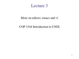
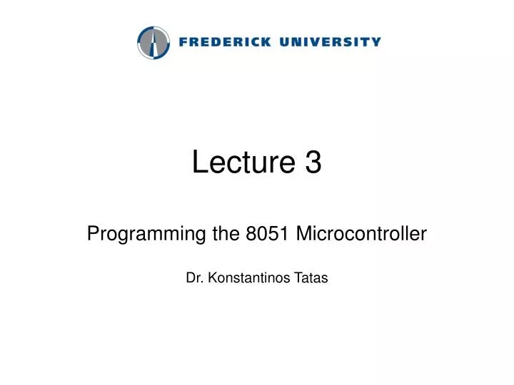
Lecture 3. Programming the 8051 Microcontroller Dr. Konstantinos Tatas. A. B. R0. DPTR. DPH. DPL. R1. R2. PC. PC. R3. Some 8051 16-bit Register. R4. R5. R6. R7. Some 8-bit Registers of the 8051 A: Accumulator B: Used specially in MUL/DIV R0-R7: GPRs. Registers.

E N D
Lecture 3 Programming the 8051 Microcontroller Dr. Konstantinos Tatas
A B R0 DPTR DPH DPL R1 R2 PC PC R3 Some 8051 16-bit Register R4 R5 R6 R7 Some 8-bit Registers of the 8051 A: Accumulator B: Used specially in MUL/DIV R0-R7: GPRs Registers ACOE343 - Embedded Real-Time Processor Systems - Frederick University
The MOV Instruction – Addressing Modes MOV dest,source ; dest = source MOV A,#72H ;A=72H MOV A, #’r’ ;A=‘r’ OR 72H MOV R4,#62H ;R4=62H MOV B,0F9H ;B=the content of F9’th byte of RAM MOV DPTR,#7634H MOV DPL,#34H MOV DPH,#76H MOV P1,A ;mov A to port 1 Note 1: MOV A,#72H ≠ MOV A,72H After instruction “MOV A,72H ” the content of 72’th byte of RAM will replace in Accumulator. 80868051 MOV AL,72H MOV A,#72H MOV AL,’r’ MOV A,#’r’ MOV BX,72H MOV AL,[BX] MOV A,72H Note 2: MOV A,R3 ≡ MOV A,3 ACOE343 - Embedded Real-Time Processor Systems - Frederick University
Arithmetic Instructions ADD A, Source ;A=A+SOURCE ADD A,#6 ;A=A+6 ADD A,R6 ;A=A+R6 ADD A,6 ;A=A+[6] or A=A+R6 ADD A,0F3H ;A=A+[0F3H] ACOE343 - Embedded Real-Time Processor Systems - Frederick University
Set and Clear Instructions SETB bit ; bit=1 CLR bit ; bit=0 SETB C ; CY=1 SETB P0.0 ;bit 0 from port 0 =1 SETB P3.7 ;bit 7 from port 3 =1 SETB ACC.2 ;bit 2 from ACCUMULATOR =1 SETB 05 ;set high D5 of RAM loc. 20h Note: CLR instruction is as same as SETB i.e: CLR C ;CY=0 But following instruction is only for CLR: CLR A ;A=0 ACOE343 - Embedded Real-Time Processor Systems - Frederick University
SUBB A,source ;A=A-source-CY SETB C ;CY=1 SUBB A,R5 ;A=A-R5-1 ADC A,source ;A=A+source+CY SETB C ;CY=1 ADC A,R5 ;A=A+R5+1 ACOE343 - Embedded Real-Time Processor Systems - Frederick University
DEC byte ;byte=byte-1 INC byte ;byte=byte+1 INC R7 DEC A DEC 40H ; [40]=[40]-1 CPL A ;1’s complement Example: MOV A,#55H ;A=01010101 B L01: CPL A MOV P1,A ACALL DELAY SJMP L01 NOP & RET & RETI All are like 8086 instructions. CALL ACOE343 - Embedded Real-Time Processor Systems - Frederick University
Logic Instructions ANL byte/bit ORL byte/bit XRL byte EXAMPLE: MOV R5,#89H ANL R5,#08H ACOE343 - Embedded Real-Time Processor Systems - Frederick University
Rotate Instructions • RR AAccumulatorrotate right • RL AAccumulator Rotate left • RRC AAccumulator Rotate right through the carry. • RLC AAccumulator Rotate left through the carry. ACOE343 - Embedded Real-Time Processor Systems - Frederick University
EDITOR PROGRAM Myfile.asm ASSEMBLER PROGRAM Myfile.lst Other obj file Myfile.obj LINKER PROGRAM Myfile.abs OH PROGRAM Myfile.hex Structure of Assembly language and Running an 8051 program ORG 0H MOV R5,#25H MOV R7,#34H MOV A,#0 ADD A,R5 ADD A,#12H HERE: SJMP HERE END ACOE343 - Embedded Real-Time Processor Systems - Frederick University
ROM memory map in 8051 family 0000H 0000H 0000H 0FFFH 1FFFH 8751 AT89C51 8752 AT89C52 7FFFH Memory mapping in 8051 4k 8k 32k DS5000-32 from Atmel Corporation from Dallas Semiconductor ACOE343 - Embedded Real-Time Processor Systems - Frederick University
7FH Scratch pad RAM 30H 2FH Bit-Addressable RAM 20H 1FH Register Bank 3 18H 17H Register Bank 2 10H 0FH (Stack) Register Bank 1 08H 07H Register Bank 0 00H • RAM memory space allocation in the 8051 ACOE343 - Embedded Real-Time Processor Systems - Frederick University
CY AC F0 RS1 RS0 OV -- P CY PSW.7 Carry flag AC PSW.6 Auxiliary carry flag -- PSW.5 Available to the user for general purpose RS1 PSW.4 Register Bank selector bit 1 RS0 PSW.3 Register Bank selector bit 0 OV PSW.2 Overflow flag -- PSW.1 User define bit P PSW.0 Parity flag Set/Reset odd/even parity RS1 RS0 Register Bank Address 0 0 0 00H-07H 0 1 1 08H-0FH 1 0 2 10H-17H 1 1 3 18H-1FH 8051 Flag bits and the PSW register • PSW Register ACOE343 - Embedded Real-Time Processor Systems - Frederick University
Instructions that Affect Flag Bits: Note: X can be 0 or 1 ACOE343 - Embedded Real-Time Processor Systems - Frederick University
Example: MOV A,#88H ADD A,#93H 88 10001000 +93 +10010011 ---- -------------- 11B 00011011 CY=1 AC=0 P=0 Example: MOV A,#38H ADD A,#2FH 38 00111000 +2F +00101111 ---- -------------- 6701100111 CY=0 AC=1 P=1 Example: MOV A,#9CH ADD A,#64H 9C10011100 +64 +01100100 ---- -------------- 100 00000000 CY=1 AC=1 P=0 ACOE343 - Embedded Real-Time Processor Systems - Frederick University
Addressing Modes • Immediate • Register • Direct • Register Indirect • Indexed ACOE343 - Embedded Real-Time Processor Systems - Frederick University
Immediate Addressing Mode MOV A,#65H MOV A,#’A’ MOV R6,#65H MOV DPTR,#2343H MOV P1,#65H Example : Num EQU 30 … MOV R0,Num MOV DPTR,#data1 … ORG 100H data1: db “Example” ACOE343 - Embedded Real-Time Processor Systems - Frederick University
Example • Write the decimal value 4 on the SSD in the following figure. Switch the decimal point off. ACOE343 - Embedded Real-Time Processor Systems - Frederick University
Register Addressing Mode MOV Rn, A ;n=0,..,7 ADD A, Rn MOV DPL, R6 MOV DPTR, A MOV Rm, Rn ACOE343 - Embedded Real-Time Processor Systems - Frederick University
Direct Addressing Mode Although the entire of 128 bytes of RAM can be accessed using direct addressing mode, it is most often used to access RAM loc. 30 – 7FH. MOV R0, 40H MOV 56H,A MOV A, 4 ; ≡ MOV A, R4 MOV 6, 2 ; copy R2 to R6 ; MOV R6,R2 is invalid ! SFR register and their address MOV 0E0H, #66H ; ≡ MOV A,#66H MOV 0F0H, R2 ; ≡ MOV B, R2 MOV 80H,A ; ≡ MOV P1,A ACOE343 - Embedded Real-Time Processor Systems - Frederick University
Register Indirect Addressing Mode • In this mode, register is used as a pointer to the data. MOV A,@Ri ; move content of RAM loc.Where address is held by Ri into A ( i=0 or 1 ) MOV @R1,B In other word, the content of register R0 or R1 is sources or target in MOV, ADD and SUBB insructions. Example: Write a program to copy a block of 10 bytes from RAM location sterting at 37h to RAM location starting at 59h. Solution: MOV R0,37h ; source pointer MOV R1,59h ; dest pointer MOV R2,10 ; counter L1: MOV A,@R0 MOV @R1,A INC R0 INC R1 DJNZ R2,L1 • jump ACOE343 - Embedded Real-Time Processor Systems - Frederick University
Indexed Addressing Mode And On-Chip ROM Access • This mode is widely used in accessing data elements of look-up table entries located in the program (code) space ROM at the 8051 MOVC A,@A+DPTR A= content of address A +DPTR from ROM Note: Because the data elements are stored in the program (code ) space ROM of the 8051, it uses the instruction MOVC instead of MOV. The “C” means code. ACOE343 - Embedded Real-Time Processor Systems - Frederick University
Example: Assuming that ROM space starting at 250h contains “Hello.”, write a program to transfer the bytes into RAM locations starting at 40h. Solution: ORG 0 MOV DPTR,#MYDATA MOV R0,#40H L1: CLR A MOVC A,@A+DPTR JZ L2 MOV @R0,A INC DPTR INC R0 SJMP L1 L2: SJMP L2 ;------------------------------------- ORG 250H MYDATA: DB “Hello”,0 END Notice the NULL character ,0, as end of string and how we use the JZ instruction to detect that. ACOE343 - Embedded Real-Time Processor Systems - Frederick University
Example: Write a program to get the x value from P1 and send x2 to P2, continuously . Solution: ORG 0 ;code segment MOV DPTR, #TAB1 ;moving data segment to data pointer MOV A,#0FFH ;configuring P1 as input port MOV P1,A L01: MOV A,P1 ;reading value from P1 MOVC A,@A+DPTR MOV P2,A SJMP L01 ;---------------------------------------------------- ORG 300H ;data segment TAB1: DB 0,1,4,9,16,25,36,49,64,81 END ACOE343 - Embedded Real-Time Processor Systems - Frederick University
External Memory Addressing • MOVX A, @R1 ; A [R1] (in external memory) • MOVX A, @DPTR • MOVX @DPTR, A ACOE343 - Embedded Real-Time Processor Systems - Frederick University
16-bit, BCD and Signed Arithmetic in 8051 Exercise: • Write a program to add n 16-bit number. Get n from port 1. And sent Sum to SSD a) in hex b) in decimal • Write a program to subtract P1 from P0 and send result to LCD • (Assume that “ACAL DISP” display A to SSD ) ACOE343 - Embedded Real-Time Processor Systems - Frederick University
MUL & DIV • MUL AB ;B|A = A*B MOV A,#25H MOV B,#65H MUL AB ;25H*65H=0E99 ;B=0EH, A=99H • MUL AB ;A = A/B, B = A mod B MOV A,#25 MOV B,#10 MUL AB ;A=2, B=5 ACOE343 - Embedded Real-Time Processor Systems - Frederick University
7FH Scratch pad RAM 30H 2FH Bit-Addressable RAM 20H 1FH Register Bank 3 18H 17H Register Bank 2 10H 0FH (Stack) Register Bank 1 08H 07H Register Bank 0 00H Stack in the 8051 • The register used to access the stack is called SP (stack pointer) register. • The stack pointer in the 8051 is only 8 bits wide, which means that it can take value 00 to FFH. When 8051 powered up, the SP register contains value 07. ACOE343 - Embedded Real-Time Processor Systems - Frederick University
0BH 0BH 0BH 0BH F3 25 12 25 12 25 0AH 0AH 0AH 0AH 09H 09H 09H 09H 08H 08H 08H 08H SP=09H SP=08H Start SP=07H SP=10H Example: MOV R6,#25H MOV R1,#12H MOV R4,#0F3H PUSH 6 PUSH 1 PUSH 4 ACOE343 - Embedded Real-Time Processor Systems - Frederick University
0BH 0BH 0BH 0BH F3 25 12 25 12 25 0AH 0AH 0AH 0AH 09H 09H 09H 09H 08H 08H 08H 08H SP=09H SP=08H Start SP=07H SP=10H Example (cont.) POP 4 POP 1 POP 6 ACOE343 - Embedded Real-Time Processor Systems - Frederick University
How to use the stack • You can use the stack as temporary storage for variables when calling functions RLC A ;you can only rotate A Call function DIV AB ; A has the wrong value!!!!! … function: MOV A, #5 ;values are for example sake MOV B, #10 MUL AB ;you can only multiply on A RET ACOE343 - Embedded Real-Time Processor Systems - Frederick University
Example (correct) RLC A ;you can only rotate A PUSH A ;saving A and B on the stack before PUSH B ;calling function Call function POP B ;restoring B POP A ;and A (POP in reverse order) DIV AB ; A has the wrong value!!!!! … function: MOV A, #5 ;values are for example sake MOV B, #10 MUL AB ;you can only multiply on A RET ACOE343 - Embedded Real-Time Processor Systems - Frederick University
Saving PSW • The Program Status Word registers contains flags that are often important for correct program flow • You can push PSW on the stack before calling a function ADD A, R0 PUSH PSW PUSH A ;saving A and R0 on the stack before PUSH R0 ;calling function Call function POP R0 ;restoring R0 POP A ;and A (POP in reverse order) POP PSW JC loop ;If this means the carry from the ;function then don’t push PSW … function: MOV A, #5 ;values are for example sake ADD A, R2 ;the flags are set according to ADD result RET ACOE343 - Embedded Real-Time Processor Systems - Frederick University
LOOP and JUMP Instructions • DJNZ: Write a program toclear ACC, then add 3 to the accumulator ten times Solution: MOV A,#0; MOV R2,#10 AGAIN: ADD A,#03 DJNZ R2,AGAING ;repeat until R2=0 (10 times) MOV R5,A ACOE343 - Embedded Real-Time Processor Systems - Frederick University
Other conditional jumps: ACOE343 - Embedded Real-Time Processor Systems - Frederick University
SJMP and LJMP: LJMP(long jump) LJMP is an unconditional jump. It is a 3-byte instruction in which the first byte is the opcode, and the second and third bytes represent the 16-bit address of the target location. The 20byte target address allows a jump to any memory location from 0000 to FFFFH. SJMP(short jump) In this 2-byte instruction. The first byte is the opcode and the second byte is the relative address of the target location. The relative address range of 00-FFH is divided into forward and backward jumps, that is , within -128 to +127 bytes of memory relative to the address of the current PC. ACOE343 - Embedded Real-Time Processor Systems - Frederick University
CJNE , JNC Exercise: Write a program that compare R0,R1. If R0>R1 then send 1 to port 2, else if R0<R1 then send 0FFh to port 2, else send 0 to port 2. ACOE343 - Embedded Real-Time Processor Systems - Frederick University
CALL Instructions Another control transfer instruction is the CALL instruction, which is used to call a subroutine. • LCALL(long call) In this 3-byte instruction, the first byte is the opcode an the second and third bytes are used for the address of target subroutine. Therefore, LCALL can be used to call subroutines located anywhere within the 64K byte address space of the 8051. ACOE343 - Embedded Real-Time Processor Systems - Frederick University
ACALL (absolute call) ACALL is 2-byte instruction in contrast to LCALL, which is 13 bytes. Since ACALL is a 2-byte instruction, the target address of the subroutine must be within 2K bytes address because only 11 bits of the 2 bytes are used for the address. There is no difference between ACALL and LCALL in terms of saving the program counter on the stack or the function of the RET instruction. The only difference is that the target address for LCALL can be anywhere within the 64K byte address space of the 8051 while the target address of ACALL must be within a 2K-byte range. ACOE343 - Embedded Real-Time Processor Systems - Frederick University
Example ACOE343 - Embedded Real-Time Processor Systems - Frederick University
I/O Port Programming Port 1(pins 1-8) • Port 1 is denoted by P1. • P1.0 ~ P1.7 • We use P1 as examples to show the operations on ports. • P1 as an output port (i.e., write CPU data to the external pin) • P1 as an input port (i.e., read pin data into CPU bus) ACOE343 - Embedded Real-Time Processor Systems - Frederick University
Read latch Vcc TB2 Load(L1) P1.X pin Internal CPU bus DQ ClkQ P1.X M1 Write to latch TB1 Read pin A Pin of Port 1 P0.x 8051 IC ACOE343 - Embedded Real-Time Processor Systems - Frederick University
Hardware Structure of I/O Pin • Each pin of I/O ports • Internal CPU bus:communicate with CPU • A D latch store the value of this pin • D latch is controlled by “Write to latch” • Write to latch=1:write data into the D latch • 2 Tri-state buffer: • TB1: controlled by “Read pin” • Read pin=1:really read the data present at the pin • TB2: controlled by “Read latch” • Read latch=1:read value from internal latch • A transistor M1 gate • Gate=0: open • Gate=1: close ACOE343 - Embedded Real-Time Processor Systems - Frederick University
Tri-state Buffer Output Input Tri-state control (active high) L H H Low L Highimpedance (open-circuit) H H ACOE343 - Embedded Real-Time Processor Systems - Frederick University
Read latch Vcc Load(L1) P1.X pin Internal CPU bus DQ ClkQ P1.X M1 Write to latch Read pin Writing “1” to Output Pin P1.X TB2 2. output pin is Vcc 1. write a 1 to the pin 1 output 1 0 TB1 8051 IC ACOE343 - Embedded Real-Time Processor Systems - Frederick University
Read latch Vcc Load(L1) P1.X pin Internal CPU bus DQ ClkQ P1.X M1 Write to latch Read pin Writing “0” to Output Pin P1.X TB2 2. output pin is ground 1. write a 0 to the pin 0 output 0 1 TB1 8051 IC ACOE343 - Embedded Real-Time Processor Systems - Frederick University
Port 1 as Output(Write to a Port) • Send data to Port 1: MOV A,#55H BACK: MOV P1,A ACALL DELAY CPL A SJMP BACK • Let P1 toggle. • You can write to P1 directly. ACOE343 - Embedded Real-Time Processor Systems - Frederick University
Reading Input v.s. Port Latch • When reading ports, there are two possibilities: • Read the status of the input pin. (from external pin value) • MOV A, PX • JNB P2.1, TARGET ; jump if P2.1 is not set • JB P2.1, TARGET ; jump if P2.1 is set • Figures C-11, C-12 • Read the internal latch of the output port. • ANL P1, A ; P1 ← P1 AND A • ORL P1, A ; P1 ← P1 OR A • INC P1 ; increase P1 • Figure C-17 • Table C-6 Read-Modify-Write Instruction (or Table 8-5) • See Section 8.3 ACOE343 - Embedded Real-Time Processor Systems - Frederick University
Read latch Vcc Load(L1) P1.X pin Internal CPU bus DQ ClkQ P1.X M1 Write to latch Read pin Reading “High” at Input Pin 2. MOV A,P1 external pin=High TB2 • write a 1 to the pin MOV P1,#0FFH 1 1 0 TB1 3. Read pin=1 Read latch=0 Write to latch=1 8051 IC ACOE343 - Embedded Real-Time Processor Systems - Frederick University