Download
1 / 32
320 likes | 475 Views
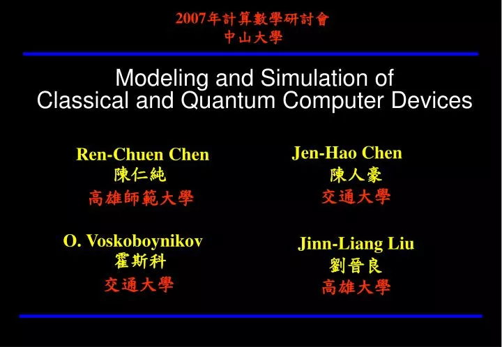
2007 年計算數學研討會 中山大學. Ren-Chuen Chen 陳仁純 高雄師範大學 O. Voskoboynikov 霍斯科 交通大學. Modeling and Simulation of Classical and Quantum Computer Devices. Jen-Hao Chen 陳人豪 交通大學 Jinn-Liang Liu 劉晉良 高雄大學. Part 1. Classical Computer. Microprocessor. Microchips. MOSFET. MOSFET

E N D
2007年計算數學研討會中山大學 Ren-Chuen Chen陳仁純 高雄師範大學 O. Voskoboynikov霍斯科 交通大學 Modeling and Simulation ofClassical and Quantum Computer Devices Jen-Hao Chen陳人豪交通大學 Jinn-Liang Liu 劉晉良高雄大學
Part 1. Classical Computer Microprocessor Microchips MOSFET
MOSFET (Metal Oxide Semiconductor Field Effect Transistor)
Semiconductor A semiconductor is a material that can behave as a conductor or an insulator depending on what is done to it. We can control the amount of current that can pass through a semiconductor. Kingfisher Science Encyclopedia
Sand Ingot Wafer Doping IC 12吋矽晶圓 Gold Ingots Silicon Ingot
Si Si Si Extra Si As Si Si Si Si - Doping Impurities (n-Type) Conducting band, Ec Ed ~ 0.05 eV Electron Eg = 1.1 eV Valence band, Ev
Conducting band, Ec Si Si Si Hole Eg = 1.1 eV Si B Si Ea ~ 0.05 eV Si Si Si - Valence band, Ev Electron Doping Impurities (p-Type)
S. Roy and A. Asenov, Science 2005 MOSFET (Metal Oxide Semiconductor Field Effect Transistor) 2003 L = 4 nm Research 2005 L = 45 nm Production 2018 L = 7 nm Production 3D, 30nm x 30nm
Gate Length: 90 nm (2005 In Production) (Device Size) 65 nm (2006 In Production) 34 nm (This Talk)
Device Sizes Vs. Models
Quantum Corrected Energy Transport Model R.-C. Chen and J.-L. Liu, JCP 2005 L=IJ=34nm
Physical Models Drift diffusion model (3 PDEs) Energy transport model (5 PDEs) Hydrodynamic Model (7 PDEs)
Energy Transport Model • the electrostatic potential • n the electron concentration • p the hole concentration • J the current density • S the energy flux • E the electric field • R the generation- recombination rate
Self-Adjoint Formulation New Variables
Adaptive Algorithm Finite Element Method Monotone Iteration Exponential Fitting
Conclusion • New Model (DGET, Self-Adjointness) • Better Approximation • Global Convergence (Monotone Iterative Method) • Efficiency • Easy Implementation