Download
1 / 92
1.19k likes | 1.81k Views
CHAPTER 5 Synchronous Sequential Logic. 5-1 Sequential Circuits. 5-2 Latches. 5-3 Flip-Flops. 5-4 Analysis of Clocked Sequential. Circuits. CHAPTER 5 Synchronous Sequential Logic. 5-5 HDL For Sequential Circuits. 5-6 State Reduction and Assignment.

E N D
CHAPTER 5 Synchronous Sequential Logic 5-1 Sequential Circuits 5-2 Latches 5-3 Flip-Flops 5-4 Analysis of Clocked Sequential Circuits
CHAPTER 5 Synchronous Sequential Logic 5-5 HDL For Sequential Circuits 5-6 State Reduction and Assignment 5-7 Design Procedure
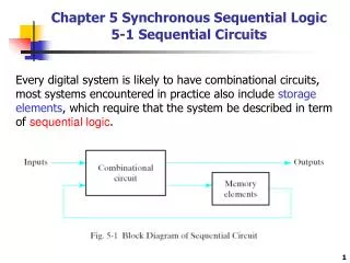
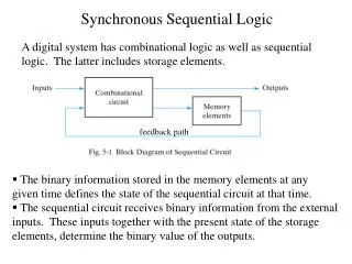
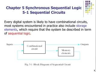
5-1 Sequential Circuits Review: Combinational Circuits: • No Storage • No Feedback • The output level is at all times dependent on the combination of input levels. Sequential Circuits: • Storage involved • Feedback involved • The output level is concerned with the prior input levels.
5-1 Sequential Circuits Sequential Circuits: The output is a function not only of the inputs, but also of the present state of the storage elements.
5-1 Sequential Circuits Synchronous Clocked Sequential Circuits Sequential Circuits: Asynchronous Sequential Circuits: Synchronous Sequential Circuits: Depends upon the input signals at any instants of time and order in which the inputs change Synchronous sequential circuits employ signals that affect the storage elements only at discrete instants of time.
5-2 Latches SR Latch A latch or flip-flop is a type of bistable logic device. Bistable devices have two stable states, called SET and RESET; they can retain either of these states indefinitely (as long as power is delivered to the circuit), making them useful as storage devices.
5-2 Latches • Basic Difference Between Latches and Flip-flops flip-flop: a sequential device that normally samples its inputs and changes its outputs only at times determined by a clocking signal. Latch: a sequential device that watches all of its inputs continuously and changes its outputs at any time, independent of a clocking signal.
5-2 Latches • The SR Latch The SR latch is a circuit with two cross-coupled NOR gates or two cross-coupled NAND gates. Two outputs are normally the complement of each other. However, when both inputs are active at the same time, an undefined state occurs.
5-2 Latches • The SR Latch with NOR Gate Function Table 1 0 1 0 1 0 0 1
5-2 Latches • The SR Latch with NOR Gate Function Table 0 1 1 0 1 0 1 0 0 1 0 1
5-2 Latches • The SR Latch with NOR Gate Function Table 0 1 1 0 1 0 0 1 0 1 0 1 1 1 0 0 It results in an unpredictable next state when both inputs return to 0.
5-2 Latches • The SR Latch with NOR Gate Function Table 1 0 1 0 1 0 0 0 0 1 0 1 1 1 0 0 0 0 1 0 (after S = 1, R = 0)
5-2 Latches • The SR Latch with NOR Gate Function Table 0 0 1 0 1 0 1 0 0 1 0 1 1 1 0 0 0 0 1 0 (after S = 1, R = 0) 0 0 0 1 (after S = 0, R = 1)
5-2 Latches • The SR Latch with NAND Gate Function Table Input signals for the NAND latch require the complement of those values used for the NOR latch.
The control input acts as an enable signal for the other two inputs. 5-2 Latches • The SR Latch with Control Input Function Table
The output of the NAND gates stays at the logic 1 as long as the control input remains at 0 5-2 Latches • The SR Latch with Control Input Function Table
This indeterminate condition means that one cannot determine the next state as it depends on whether the S or R input goes to 0 first. 5-2 Latches • The SR Latch with Control Input Function Table
5-2 Latches • D Latch 1 No indeterminate state 0 1 As long as the control input is at 0, the circuit cannot change state regardless of the value of D.
5-2 Latches • D Latch 1 0 1 1 0 1 0 The D input is sampled when C = 1.
5-2 Latches • D Latch 0 1 Function Table 0 1 1 0 1 The D input is sampled when C = 1.
5-3 Flip - Flops If the inputs applied to the latches change while the clock pulse is still in the active level, the latch will respond to new value. The result is unpredictable. The key to the proper operation of a flip-flop is to trigger it only during a signal transition.
5-3 Flip - Flops • Edge-Triggered D Flip-Flop 1 0 When the clock (CLK) is 1, the data from the D input is transfer to the master. The slave is disabled.
5-3 Flip - Flops • Edge-Triggered D Flip-Flop 0 1 When the clock (CLK) return to 0, the master is disabled. The value of Y is transferred to the output of flip-flop at Q.
5-3 Flip - Flops • Edge-Triggered D Flip-Flop When the clock (CLK) = 0, the S and R are maintained at 1. Output remains in its present state. 1 0 1
0 1 0 1 5-3 Flip - Flops • Edge-Triggered D Flip-Flop If D = 0 when the clock (CLK) becomes 1, R changes to 0. 0 1 1 1 1 0 0 If D changes while CLK = 1, R remains at 0. 1 0 1 1 0
5-3 Flip - Flops • Edge-Triggered D Flip-Flop In summary, when the input clock in the positive-edge-triggered flip-flop makes a positive transition, the value of D is transferred to Q. A negative transition and steady logic 1 or 0 level do not affect the output. Graphic Symbol for Negative-Edge-Triggered D Flip-Flop Graphic Symbol for Positive-Edge-Triggered D Flip-Flop
5-3 Flip - Flops • Other Flip-Flops The edge-triggered D Flip-Flopisthe most economical and efficient because it requires the smallest number of gates. Other types of flip-flop can be constructed by using the D Flip-Flop and external logic.
5-3 Flip - Flops • Other Flip-Flops Circuit diagram of JK Flip-Flop JK Flip-Flop The logic expression of JK Flip-Flop is Graphic symbol of JK Flip-Flop Q = D = JQ' + K'Q
5-3 Flip - Flops • Other Flip-Flops Circuit diagram of T Flip-Flop The logic expression of T Flip-Flop is T Flip-Flop The dynamic indicator denotes that the flip-flop responds to the edge transition of the clock Graphic symbol of T Flip-Flop Q = D = TQ' + T'Q
5-3 Flip - Flops • Characteristic Tables
5-3 Flip - Flops • Characteristic Equations Characteristic equation for D flip-flop Q(t+1) = D Characteristic equation for JK flip-flop Q(t+1) = JQ' + K'Q Characteristic equation for T flip-flop Q(t+1) = TQ' + T'Q
5-3 Flip - Flops • Direct Inputs It is useful for bringing all flip-flops in the system to a known starting state prior to the clocked operation Function Table of a D Flip-flop with Asynchronous Reset The input that sets the flip-flop to 1 is called preset or direct set. Graphic Symbol of a D Flip-flop with Asynchronous Reset The input that clears the flip-flop to 0 is called clear or direct reset.
5-3 Flip - Flops • Direct Inputs Asynchronous Reset of D flip-flop 1 0 1 1 0
5-4 Analysis of Clocked Sequential Circuits • State Equations A(t+1) = A(t) x(t) + B(t) x(t) B(t+1) = A'(t) x(t) A state equation ( also called transition equation) specifies the next state as a function of the present state and inputs. The compact form A(t+1) = Ax + Bx B(t+1) = A'x
5-4 Analysis of Clocked Sequential Circuits Output Expression y(t) = [A(t) + B(t)] x'(t) The compact form y = [A + B] x'
5-4 Analysis of Clocked Sequential Circuits • State Table Listing all possible binary combinations of present state and inputs
5-4 Analysis of Clocked Sequential Circuits • State Table The next state of flip-flop A must satisfy the state equation.
5-4 Analysis of Clocked Sequential Circuits • State Table The output must satisfy the output equation.
The binary number inside each circle identifies the state of the flip-flops. 5-4 Analysis of Clocked Sequential Circuits • State Diagram
The input value during the present state is labeled first, and the number after the slash gives the output. 5-4 Analysis of Clocked Sequential Circuits • State Diagram It is more suitable for human interpretation of the circuit operation
5-4 Analysis of Clocked Sequential Circuits • Flip-Flop Input Equations Two flip-flop input equations and an output equation: DA = Ax + Bx DB = A'x y = ( A + B )x'
5-4 Analysis of Clocked Sequential Circuits State table • Analysis with D Flip-Flop Input Equation : DA = A ⊕ x ⊕ y The next state value: A = A ⊕ x ⊕ y
5-4 Analysis of Clocked Sequential Circuits State Diagram • Analysis with D Flip-Flop • The procedure for analysis with JK Flip-Flop and with D Flip-Flop is similar.
5-4 Analysis of Clocked Sequential Circuits • Mealy and Moore Models In the Mealy model, the output is a function of both the present state and input. Output y is a function of both input x and the present state of A and B.
5-4 Analysis of Clocked Sequential Circuits • Mealy and Moore Models In the Moore model, the output is a function of the present state only. An example of Moore model
5-5 HDL for Sequential Circuits The always behavior executes repeatedly and reexecutes until the simulation terminates. The initial behavior executes once beginning at time = 0 • Behavioral Modeling Two kinds of behavioral statement: initial and always Example 1: Clock is complemented every 10 time units and is repeated 30 times. Initial begin clock = 1'b0 ; repeat (30) #10 clock = ~ clock; end
5-5 HDL for Sequential Circuits • Behavioral Modeling Example 2: Initial begin clock = 1'b0 ; #300 $finish end always #10 clock = ~ clock; The simulation terminates in response to the $finishsystem task at time 300.
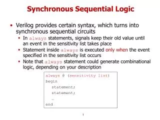
5-5 HDL for Sequential Circuits • Behavioral Modeling The always statement: always @ ( event control expression ) Procedural assignment statements. The event control expression specifies the condition that must occur to activate the execution of the procedural assignment statement.
5-5 HDL for Sequential Circuits • Behavioral Modeling The always statement: always @ ( event control expression ) Procedural assignment statements. The variables in the left-hand side of the procedural statements must be of the reg data type.
The first statement transfers A into B. 5-5 HDL for Sequential Circuits • Behavioral Modeling Two kinds of procedural assignment: blocking and non-blocking Example of blocking assignment B = A C = B + 1