Download
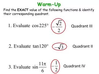
1 / 23
300 likes | 554 Views
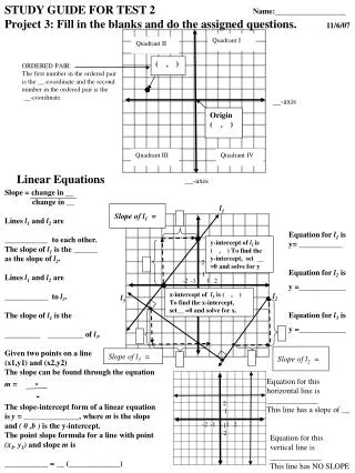
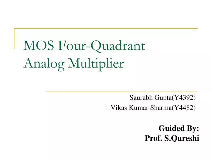
MOS Four-Quadrant Analog Multiplier. Saurabh Gupta(Y4392) Vikas Kumar Sharma(Y4482). Guided By: Prof. S.Qureshi. Introduction. Various Applications Modulation Demodulation Wave Shaping Many Designs have limitations of two-quadrant multiplication only. Concept.

E N D
MOS Four-Quadrant Analog Multiplier Saurabh Gupta(Y4392) Vikas Kumar Sharma(Y4482) Guided By: Prof. S.Qureshi
Introduction • Various Applications • Modulation • Demodulation • Wave Shaping • Many Designs have limitations of two-quadrant multiplication only
Concept • The basic motivation behind the design is : • This have been a favorite of analog multiplier designs but has its own limitations (later)
MOS Properties • MOSFET’s have the special property of squaring current in saturation • This can be exploited to make the sum/difference Squaring Circuits.
Design • The design has two major parts : • Sum-Squaring Circuit • Difference-Squaring Circuit • The difference of the two outputs gives the multiplication with some constant gain
Design Equations • Output Voltage -> • Max. Input voltage (for linear operation)
Conclusion • The circuit is found to be working satisfactorily for differential input voltages up to 0.5 V • The Circuit is found to have a -0.2dB gain drop at 1 Ghz(suited for high frequency applications) • It is sensitive to component mismatch
Limitations • Body-effect neglected in the design • CLM modifies the behavior from expected • Component Mismatch will result in harmonic impurity
Acknowledgement We are thankful to Dr. Qureshi for giving us this opportunity and to our TA’s who were always there for helping us out.
References • “An MOS Four-Quadrant Analog Multiplier Using Simple Two-Input Squaring Circuits with Source Followers” by Ho-Jun Song & Choong-Ki Kim, IEEE JOURNAL OF SOLID-STATE CIRCUITS, VOL. 25, NO. 3, JUNE 1990