Download
1 / 1
10 likes | 141 Views
Single crystalline Tm 2 O 3 film grown on Si (100) by atomic oxygen assisted molecular beam epitaxy. T. Ji 1 , J. Cui 1 , Y. L. Fan 1 , Z. B. Fang 2 and Z. M. Jiang 1 1 State Key Laboratory of Surface Physics, Fudan University, Shanghai 200433, China

E N D
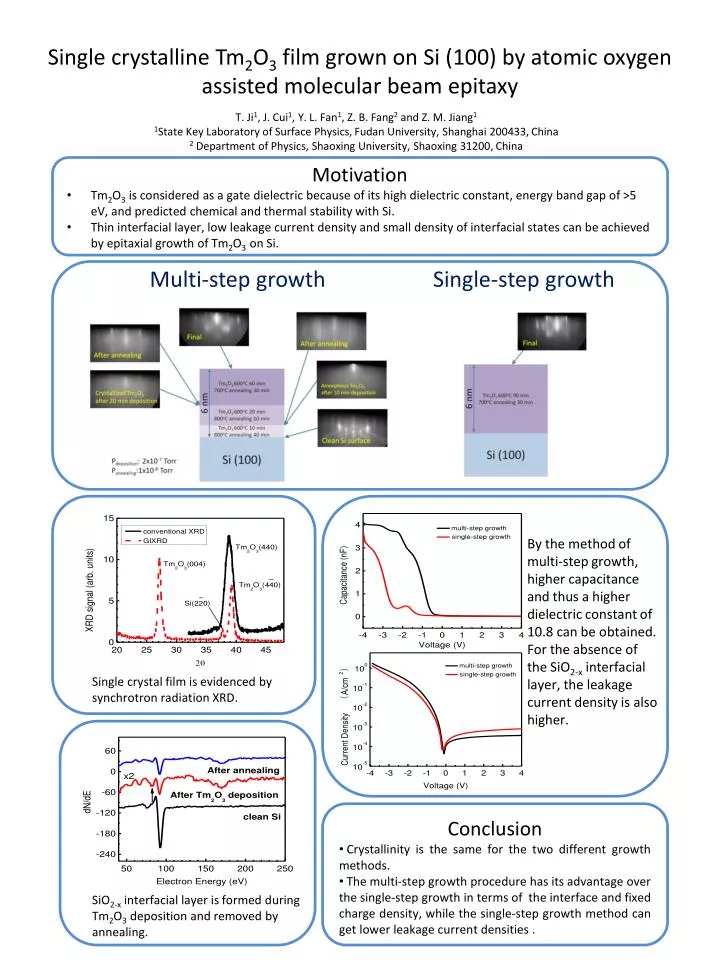
Single crystalline Tm2O3 film grown on Si (100) by atomic oxygen assisted molecular beam epitaxy T. Ji1, J. Cui1, Y. L. Fan1, Z. B. Fang2 and Z. M. Jiang1 1State Key Laboratory of Surface Physics, Fudan University, Shanghai 200433, China 2 Department of Physics, Shaoxing University, Shaoxing 31200, China • Motivation • Tm2O3 is considered as a gate dielectric because of its high dielectric constant, energy band gap of >5 eV, and predicted chemical and thermal stability with Si. • Thin interfacial layer, low leakage current density and small density of interfacial states can be achieved by epitaxial growth of Tm2O3on Si. Multi-step growth Single-step growth 11 By the method of multi-step growth, higher capacitance and thus a higher dielectric constant of 10.8 can be obtained. For the absence of the SiO2-x interfacial layer, the leakage current density is also higher. Single crystal film is evidenced by synchrotron radiation XRD. • Conclusion • Crystallinityis the same for the two different growth methods. • The multi-step growth procedure has its advantage over the single-step growth in terms of the interface and fixed charge density, while the single-step growth method can get lower leakage current densities . SiO2-x interfacial layer is formed during Tm2O3 deposition and removed by annealing.