Download
1 / 6
60 likes | 263 Views
Final Lab. Objectives Presentation Time Slot Logistics Team Option Final Presentation Dry Run ~1:45 (P4) or ….. Prototyping – Report Assembly Time Tuesday DEC 12 – Tentative Schedule for EMS-W220 Team 1: 8:30 – 10:20AM Team 2: 10:30 – 12:20PM Team 3: 1:30 – 3:20PM

E N D
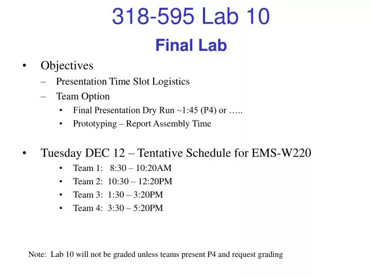
Final Lab • Objectives • Presentation Time Slot Logistics • Team Option • Final Presentation Dry Run ~1:45 (P4) or ….. • Prototyping – Report Assembly Time • Tuesday DEC 12 – Tentative Schedule for EMS-W220 • Team 1: 8:30 – 10:20AM • Team 2: 10:30 – 12:20PM • Team 3: 1:30 – 3:20PM • Team 4: 3:30 – 5:20PM Note: Lab 10 will not be graded unless teams present P4 and request grading
Suggested Final Slide Order • Project Definition & System Design • All Project Proposals including block diagrams (Appendix) • Selection Process including systematic scoring system (Appendix) • Recommended Project – Summary Page • Refined Block Diagram • Perf Requirements Summary – Showcase Key Requirements • Std Requirements Summary – Showcase Key Requirements • Product Safety Requirements/Standards Summary Slide(s) – Lab 2A • Product EMC Requirements/Standards Summary Slide(s) – Lab 2B • Basic Business Case • Block Diagram Description Page • Requirements Spreadsheet: Project Level Tabs (Excel File – Appendix) • Requirements Spreadsheet: Block Level Tab Flowdowns (Excel File – App) • Key Risk Areas • 3 Key Patents (IP) Found for Product Area Labs 1A-B Lab 1C
Suggested Final Slide Order • Project Detailed Design • Product Level Design Plan Summary & Gantt Chart Slides – Lab 3 • Overall Prototype Plan – Lab3 • Product Overall Reliability Rollup Summary Slide(s), Final Warranty – Lab 4 • Product Overall Reliability Growth Plan (Optional) Slide(s) – Lab 4 • Product Overall Mfg Assembly and Test Process Diagram – Lab 6 • User Manual (show a few key pages or hilights) – Lab 9 • Overall Integration and Lab Testing – Demo Setup Insert Block Design Slides Here
Suggested Slide Order for Design Blocks • Block Design Slides • Block Description and Purpose Slide(s) – P2 • Include location of Block in overall block diagram, Describe Purpose of Block • Block Performance & Standard Requirements Summary – P3 • Include ALL Safety, EMC and Reliability Requirements • Show All % Allocations from Product Level • Block Breakdown Diagram Slide (Block Diag of the Block) – P2 • Block Signal Input/Output Summary Slide(s) – Lab 2A • Block Prototype Schematic – Lab 3 • 5-6 Bullets Describing Theory of Operation
Suggested Slide Order for Design Blocks Block Design Slides Continued • Detailed Design Calculations & Component Selections – P3 • Show all Calculations and Selection Rationale for ALL Components and Their Attributes • Device Package Type Rationale • Nominal Resistance, Capacitance, Inductance Values & % Tolerance Calculations • Resistor Compositions, Capacitor Dielectric, Inductor Winding; Selection Rationale • Resistor, Capacitor, Inductor, Diode, Transistor & IC Max Voltage Calculations • Resistor, Inductor, Transistor, Diode, Xfmr, & IC Max Power Calculations • Power Electronics Heat Sink qj Calculations and Max Die Temp Rise Above Ambient • EMC Devices including filters, ferrites, transient absorbers, etc • Safety Devices such as Current Limiters incl Fuses, Breakers, GFCI, etc • Wire Gauges, Interconnect Contact, & Trace Width Ratings • Op-Amp Selections including Ib, Vio, CMRR, Slew Rate, Iout & Error Voltage Calculations • Logic Family Selection including Interface Compatibility, Speed, Power • CPU and/or PLD Types and Clock Speed, Performance Capabilities • Regulator Basic Performances incl % line and % load regulations • Nominal Time Domain Operational Simulations • Nominal Frequency Domain Operational Simulations • Worst Case or Monte-Carlo Simulations • Additional Analog Circuit DFM Analysis as applicable • Additional Digital Circuit DFM Analysis as applicable (Lab 8) • Additional Power Circuit DFM Analysis as applicable (Lab 8) • Firmware & Programming Design Descriptions as applicable • Flow Charts • State Diagrams and Bubble Charts • Description of Development Tools and Environment • Configurations and Setup
Suggested Slide Order for Design Blocks Block Design Slides Cont • Block Prototype BOM – Lab 3 • Block Production BOM – Lab 5 • Block Prototype Netlist – Lab 3 • Block Prototype Layout – Lab 3 • Block Production Schematic, Netlist & Layout (Optional)– Lab 5 • Block Parts Count Reliability Estimation Slide – Lab 4 • Block Life Cycle Obsolescence Analysis– Lab 9 • Block Prototype Lab Verification Results • Dig O-scope ePictures • Dig Photos of Prototype • Dig Photos of Laboratory Testing • Dig Videos of Laboratory Testing