Download
1 / 64
650 likes | 804 Views
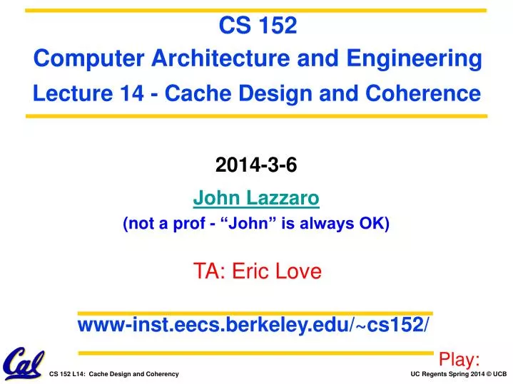
www-inst.eecs.berkeley.edu/~cs152/. CS 152 Computer Architecture and Engineering. Lecture 14 - Cache Design and Coherence. 2014-3-6 John Lazzaro (not a prof - “John” is always OK). TA: Eric Love. Play:. Today: Shared Cache Design and Coherence. CPU multi-threading

E N D
www-inst.eecs.berkeley.edu/~cs152/ CS 152 Computer Architecture and Engineering Lecture 14 - Cache Design and Coherence 2014-3-6 John Lazzaro (not a prof - “John” is always OK) TA: Eric Love Play:
Today: Shared Cache Design and Coherence CPU multi-threading Keeps memory system busy. ... CPU CPU Private Cache Private Cache Crossbars and Rings How to do on-chip sharing. ... Shared Caches Concurrent requests Interfaces that don’t stall. DRAM Coherency Protocols Building coherent caches. Shared Ports I/O
Sun Microsystems Niagara series Multithreading
The case for multithreading Amdahl’s Law tells us that optimizing C is the wrong thing to do ... Some applications spend their lives waiting for memory. C = compute M = waiting Idea: Create a design that can multiplex threads onto one pipeline. Goal: Maximize throughput of a large number of threads.
Labels show this state: T4 T3 T2 T1 Multi-threading: Assuming perfect caches 4 CPUs, running @ 1/4 clock. S. Cray, 1962.
Result: Critical path shortens -- can trade for speed or power. Bypass network is no longer needed ... ID (Decode) EX WB MEM IR IR IR IR WE, MemToReg From WB Mux,Logic A Y R M M B
A thread scheduler keeps track of information about all threads that share pipeline. When a thread experiences a cache miss, it is taken off the pipeline during the miss penalty period. Thread scheduler Multi-threading: Supporting cache misses
Sun Niagara II # threads/core? 8 threads/core: Enough to keep one core busy, given clock speed, memory system latency, and target application characteristics.
Shared-memory CPUs share lower level of memory system, and I/O. ... CPU CPU Common address space, one operating system image. Private Cache Private Cache ... Shared Caches Communication occurs through the memory system (100ns latency, 20 GB/s bandwidth) DRAM Shared Ports I/O
Sun’s Niagara II: Single-chip implementation ... SPC == SPARC Core. Only DRAM is not on chip.
clk sel(rs1) sel(ws) Q R0 - The constant 0 5 5 32 ... MUX 32 En Q D R1 DEMUX rd1 WE ... En Q D R2 32 ... sel(rs2) ... 5 32 ... MUX En 32 R31 Q D rd2 32 32 wd Crossbar: Like N ports on an N-register file Flexible, but ... reads slowsdown as O(N2) ... Why? Number of loads on each Q goes as O(N), and the wire length to port mux goes as O(N).
Design challenge: High-performance crossbar Each DRAM channel: 50 GB/s Read, 25 GB/s Write BW. Crossbar BW: 270 GB/s total (Read + Write). Niagara II: 8 cores, 8 L2 banks, 4 DRAM channels. Apps are locality-poor. Goal: saturate DRAM BW.
Sun Niagara II 8 x 9 Crossbar Tri-state distributed mux, as in microcode talk. Every cross of blue and purple is a tri-state buffer with a unique control signal. 72 control signals (if distributed unencoded).
Sun Niagara II 8 x 9 Crossbar 8 ports on CPU side (one per core) 4 cycle latency (715ps/cycle). Cycles 1-3 are for arbitration. Transmit data on cycle 4. 100-200 wires/ port (each way). 8 ports for L2 banks, plus one for I/0 Pipelined.
Epoch 2: Allocation algorithm decides which inputs get to write. Epoch 3: Allocation system informs the winning inputs and outputs. Epoch 4: Actual data transfer takes place. A complete switch transfer (4 epochs) Epoch 1: All input ports (that are ready to send data) request an output port. Allocation is pipelined: a data transfer happens on every cycle, as does the three allocation stages, for different sets of requests.
Allocator returns a matrix with at most one 1 in each row and column to set switches. Algorithm should be “fair”, so no port always loses ... should also “scale” to run large matrices fast. Epoch 3: The Allocation Problem (4 x 4) Output Ports (W, X, Y, Z) A 1 codes that an input has data ready to send to an output. Input Ports (A, B, C, D)
Sun Niagara II Crossbar Notes Low latency: 4 cycles (less than 3 ns). Uniform latency between all port pairs. Crossbar defines floorplan: all port devices should be equidistant to the crossbar.
Sun Niagara II Energy Facts Crossbar only 1% of total power.
Sun Niagara II Crossbar Notes Low latency: 4 cycles (less than 3 ns). Uniform latency between all port pairs. Crossbar defines floorplan: all port devices should be equidistant to the crossbar. Did not scale up for 16-core Rainbow Falls. Rainbow Falls keeps the 8 x 9 crossbar, and shares each CPU-side port with two cores. Design alternatives to crossbar?
CLOS Networks: From telecom world ... Build a high-port switch by tiling fixed-sized shuffle units. Pipeline registers naturally fit between tiles. Trades scalability for latency.
CLOS Networks: An example route Numbers on left and right are port numbers. Colors show routing paths for an exchange. Arbitration still needed to prevent blocking.
Intel Xeon Data Center server chip 20% of Intel’s revenues, 40% of profits. Why? Cloud is growing, Xeon is dominant.
Compiled Chips Ring Bus Xeon is a chip family, varying by # of cores, L3 cache size. Chip family mask layouts generated automatically, by adding core/cache slices.
Bi-directional Ring Bus connects: Cores, cache banks, DRAM controllers, off-chip I/O. Ring Stop Chip compiler might size the ring bus to scale bandwidth with # of cores. Ring latency increases with # of cores. But compared to baseline, small.
Tiles along x-axis are 20 ways of cache 2.5 MB L3 cache slice from Xeon E5 Ringstop interface lives in the Cache Control Box (CBOX)
Ring bus (perhaps 1024 wires), with address, data, and header fields (sender #, recipient #, command) Ring Stop #3 Ring Stop #1 Ring Stop #2 Empty Data Out Data In Control Ring Stop #2 Interface 1024 Reading: Sense Data Out to see if message is for Ring Stop #2. If so, latch data, mux Empty onto ring. Writing: Check is DataOut is Empty. If so, mux a message onto the ring via the DataIn port.
In practice: “Extreme EE” to co-optimize bandwidth, reliability.
Debugging: “Network analyzer” built into chip to capture ring messages of a particular kind. Sent off chip via an aux port.
A derivative of this ring bus is also used on laptop and desktop chips.
Break Play:
Recall: CPU-cache port that doesn’t stall on a miss CPU makes a request by placing the following items in Queue1: Queue 1 Queue 2 CMD: Read, write, etc ... MTYPE: 8-bit, 16-bit, 32-bit, or 64-bit. TAG: 9-bit number identifying the request. MADDR: Memory address of first byte. STORE-DATA: For stores, the data to store. From CPU To CPU
This cache is used in an ASPIRE CPU (Rocket) From CPU To CPU When request is ready, cache places the following items in Queue2: Queue 1 Queue 2 TAG: Identity of the completed command. LOAD-DATA: For loads, the requested data. CPU saves info about requests, indexed by TAG. Why use TAG approach? Multiple misses can proceed in parallel. Loads can return out of order.
Today: How a read request proceeds in L1 D-Cache Queue 1 Queue 2 From CPU To CPU CPU requests a read by placing MTYPE, TAG, MADDR in Queue 1. “We” == L1 D-Cache controller We do a normal cache access. If there is a hit, we put place load result in Queue 2 ... In the case of a miss, we use the Inverted Miss Status Holding Register.
= = Inverted MSHR (Miss Status Holding Register) (1) Associatively look up block # of memory address in table. If there are no hits, do memory request. To look up a memory address ... Cache Block # Tag ID (ROM) 1st Byte in Block Valid Bit MTYPE 8 0 42 0 1 0 4 0 512-entry table, so that every9-bitTAGvalue has an entry. Valid Qualifies Hit Hit [ ... ] [ ... ] Assumptions: 32-byte blocks, 48-bit physical address space. Hit Valid Qualifies Hit
(2) Index into table using 9-bit TAG, and set all fields using MADDR and MTYPE queue values. = = 8 0 Inverted MSHR (Miss Status Holding Register) This indexing always finds V=0, because CPU promises not to reuse in-flight tags. To look up a memory address ... Cache Block # Tag ID (ROM) 1st Byte in Block Valid Bit MTYPE 8 0 42 0 1 0 4 0 512-entry table, so that every9-bitTAGvalue has an entry. Valid Qualifies Hit Hit [ ... ] [ ... ] Assumptions: 32-byte blocks, 48-bit physical address space. Hit Valid Qualifies Hit
= = Inverted MSHR (Miss Status Holding Register) (3) Whenever memory system returns data, associatively look up block # to find allpendingtransactions. Place transaction data for all hits in Queue 2, and clear valid bits. Also update L1 cache. To look up a memory address ... Cache Block # Tag ID (ROM) 1st Byte in Block Valid Bit MTYPE 8 0 42 0 1 0 4 0 512-entry table, so that every9-bitTAGvalue has an entry. Valid Qualifies Hit Hit [ ... ] [ ... ] Assumptions: 32-byte blocks, 48-bit physical address space. Hit Valid Qualifies Hit
Inverted MHSR notes. Structural hazards only occur when TAG space is exhausted by the CPU. High cost (# comparators + SRAM cells). See Farkas and Jouppi on class website, for low-cost designs that are often good enough. We will return to MHSRs to discuss CPI performance later in the semester.
CPU1: CPU1: CPU0: SW R0,16(R0) LW R2, 16(R0) LW R2, 16(R0) 0 16 5 0 16 5 Two CPUs, two caches, shared DRAM ... CPU1 CPU0 View of memory no longer “coherent”. Loads of location 16 from CPU0 and CPU1 see different values! Today: What to do ... 5 Write-through caches
The simplest solution ... one cache! CPUs do not have internal caches. Only one cache, so different values for a memory address cannot appear in 2 caches! CPU1 CPU0 Multiple caches banks support read/writes by both CPUs in a switch epoch, unless both target same bank. In that case, one request is stalled.
This approach was a complete solution in the days when DRAM row access time and CPU clock period were well matched. Sequent Systems (1980s) Not a complete solution ... good for L2. For modern clock rates, access to shared cache through switch takes 10+ cycles. CPU1 CPU0 Using shared cache as the L1 data cache is tantamount to slowing down clock 10X for LWs. Not good.
Modified form: Private L1s, shared L2 Thus, we need to solve the cache coherency problem for L1 cache. CPU0 CPU1 L1 Caches L1 Caches Advantages of shared L2 over private L2s: Processors communicate at cache speed, not DRAM speed. Constructive interference, if both CPUs need same data/instr. Disadvantage: CPUs share BW to L2 cache ...
IBM Power 4 (2001) Dual core Shared, multi-bank L2 cache. Private L1 caches Off-chip L3 caches
Cache coherency goals ... CPU1 CPU0 1. Only one processor at a time has write permission for a memory location. 2. No processor can load a stale copy of a location after a write. 16 5 16 5 0 0 5