Download
1 / 10
100 likes | 285 Views
ECE-C302 Bit-serial Multiplication Part 1 Prawat Nagvajara. Bit-serial Multiplication Mapping Dependency Graph onto Signal Flow Graph (DG => SFG) A schedule that implies N-bit Adder Reading. Serial Bit-vector Multiplication. Two nested-loop Algorithm For I in 0 to n-1 loop

E N D
ECE-C302Bit-serial MultiplicationPart 1Prawat Nagvajara • Bit-serial Multiplication • Mapping Dependency Graph onto Signal Flow Graph (DG => SFG) • A schedule that implies N-bit Adder • Reading
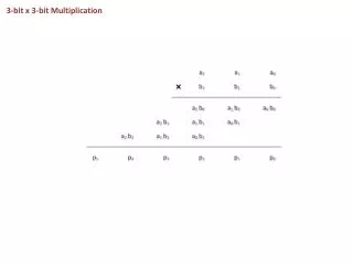
Serial Bit-vector Multiplication • Two nested-loop Algorithm For I in 0 to n-1 loop For J in 0 to n-1 loop … End loop; End loop; • Compute inner loop using combination N-bit adder and iterate Outer loop in time • It will take N clock cycles to complete • Array multiplier does not work with clock. It is a combinational circuit
A Version of Serial Multiplier (a0,a1,a2,a3,a4) Partial Sum b0, b1, …, b4 Serially AND gates carry N-bit Adder P0, P1, …, P4 serially Register
DG => SFG • SFG dimension less than DG due to iteration in time • We often linear project DG to obtain SFG, e.g., a line to a point in the adder example • How do we compute the DG? • Hyper plane of computations done at each clock cycle • Schedule for the nodes. When and where they are computed
Mapping Multiplication DG onto an SFG t = 0 t = 1 t = 2 t = 3 t = 4 carry b(t) D D D D D p(t)
Processing Element X_j Y_i AND Full Adder C_out C_in DFF PS_in PS_out CK
Another Version of Serial Multiplier x4 x3 x2 x1 x0 b0,…,b4 ‘0’ p0,p1,… Application Note: When t = 0, 1, 2, 3, 4 apply b0, b1, b2, b3, b4; When t = 5, 6, 7, 8, 9 apply ‘0’, to flush out p4, p5, …, p9
Closing Remarks • Reading • Bhasker Section 4.17 pp 98-100