Download
1 / 23
230 likes | 384 Views
NUMEXO2 Mother Board Design Status Exogam Collaboration. Abderrahman BOUJRAD GANIL France. Agenda NUMEXO2_P1 Design goals Status NUMEXO2_P2 Introduction Block diagrams Status. EXOGAM2. NUMEXO2_P1-Design Goals. Early prototype: NUMEXO2 Phase 1

E N D
NUMEXO2 Mother Board Design StatusExogam Collaboration Abderrahman BOUJRAD GANIL France
Agenda NUMEXO2_P1 Design goals Status NUMEXO2_P2 Introduction Block diagrams Status EXOGAM2
NUMEXO2_P1-Design Goals • Early prototype: NUMEXO2 Phase 1 • a simple digitizer (14 bits /100MHz) without GTS • The design goals were essentially three fold: • Validation of the critical components, particularly the FADC Ads6244 • Validation of the PowerPC architecture for Slow Control and data readout flow • Testing and validation of the analysis tools developed by the GAP (Groupe d’Acquisition pour la Physique)
NUMEXO2_P1 The NIM digitizer prototype (phase1)
NUMEXO2_P1 - Status • Better Knowledge on PowerPC Architecture & Embedded Linux • Peripherals: SRAM, SDRAM, Flash, SPI, UART, Ethernet • Conversion chain (14b / 100 MHz & 200 MHz) validated • 14b / 100 Mhz, NUMEXO2_P1 • 14b / 200Mhz, ML605 Xilinx Evaluation Kit for NEDA • Vigru (Analysis tools) validated • Energy Algorithms (MWD) & trigger concept validated • Knowledge on high speed serial links validated
NUMEXO2_P2-Introduction NUMEXO2 Phase 2 (NUMEXO2_P2) : full digitizer & GTS implementation 16 Channels digital conversion system Mezzanine card concept more flexibility Up to 16 Triggers,Time Stamping and Clock tree PCI Express (4x) for NEDA and ADONIS High counting rate ( 50 to 100 KHz)
NUMEXO2_P2-Introduction • NUMEXO2 phase 2 started on February 24, 2011 • The Architecture is now completely defined • CAD was shared between the different contributors : • GANIL, IPNO, IFJPAN • Firmware developments : • PCIexpress , IP_oscilloscope IPNO / Orsay • ADC_Interface_IP HIL / Warsaw • Gts_leaf_IP IFJPAN / krakow
Serial PCIe Ethernet link (4 Lane) Gigabit Flash PROM PPC (Linux) (VHDL) Common Logic DDR2 Optical GTS Fanin ADC Logic Interface Mux Link Clocks RAW DATA (event parameters) Samples Delay (Local & FIFO Line Recovered) DACs ADC Logic (Test, control, - FADC samples collection inspection) - Digital Processing 4 2*FADC - Trigger PROM 14 bits - Data formatting - Inspection control (VHDL) 200MHz -------- NUMEXO2_P2- Bloc Diagram
NUMEXO2_P2 Virtex5 Block diagram GANIL Caen IPNO Orsay IUAC New Delhi IFJPAN krakow HIL Warsaw
GTS Paralleldata PCIe Iserdes GTS FIFO_PCIe FIFO_PCIe FIFO_PCIe GTS NUMEXO2_P2 assignment of Virtex5 banks Preliminary
NUMEXO2_P2 Virtex6 Block diagram GANIL Caen IPNO Orsay
NUMEXO2_P2-Firmware Status The architecture is approved Elements such as the DDR2, the flash, Ethernet, PCI Express 8X (developed by IPNO), the serial bus (RS232, SPI and IIC) and the serial link for data recovery for NEDA and ADONIS were implemented in the PPC440 architecture It remains the implementation of GTS and data readout on V5: GTS IPs (Global Trigger Systems, Dulny & Czermak / IFJPAN) Clock recovery IP developed by ET (IUAC) Data readout IP (Radeck, HIL)
NUMEXO2_P2 - CAD Status 90 % of CAD is done but need to be verified : The embedded Linux CAD (DDR2,Flash, ethernet…) associated to the PPC 440 is done GANIL The CAD for the GTS features GANIL & IFJPAN The CAD associated to the Virtex6 and its peripherals is done GANIL CAD of PCI Express and its peripherals IPNO CAD of power management almost finished GANIL
NUMEXO2_P2 V6 Firmware Principal IPs => validated on numexo2_P1 & on the Xilinx ML605 evaluation kit RTL view from SYNPLIFY PRO synthesis tool ISERDES Energy Embedded Histogram
NUMEXO2_P2 – Energy visualisation Embedded logic analyser • s = 1.3 • 1 LSB = 0.802 mV
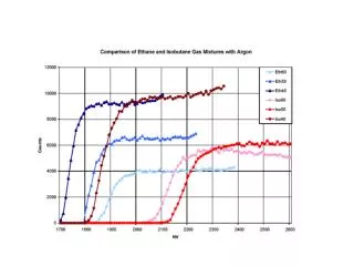
NUMEXO2_P2 - Co60 spectrum FADC 14 bits @ 250MHz + MWD ADS62P49@250MHz CSP output MWD output CM2DM signal box ML605 Co60 source spectrum FWHM = 2.7 keV @ 1.3 MeV EXOGAM clover
NUMEXO2_P2-Digital TDC TEST BENCH
NUMEXO2_P2 - Digital TDC Resolution obtained with the vernier alone without the DFC
NUMEXO2_P2- Front and Back sides FRONT SIDE BACK SIDE
NUMEXO2_P2- mother card Implementation The implementation of the components on the motherboard is in progress BACK SIDE FRONT SIDE