Download
1 / 1
10 likes | 185 Views
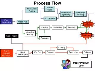
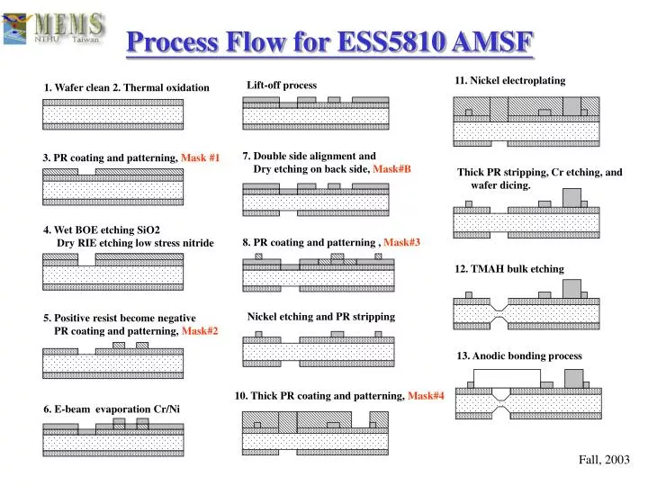
Process Flow for ESS5810 AMSF. 11. Nickel electroplating. Lift-off process. 1. Wafer clean 2. Thermal oxidation. 7. Double side alignment and Dry etching on back side, Mask#B. 3. PR coating and patterning, Mask #1. Thick PR stripping, Cr etching, and wafer dicing.

E N D
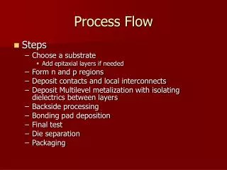
Process Flow for ESS5810 AMSF 11. Nickel electroplating Lift-off process 1. Wafer clean 2. Thermal oxidation 7. Double side alignment and Dry etching on back side, Mask#B 3. PR coating and patterning, Mask #1 Thick PR stripping, Cr etching, and wafer dicing. 4. Wet BOE etching SiO2 Dry RIE etching low stress nitride 8. PR coating and patterning , Mask#3 12. TMAH bulk etching Nickel etching and PR stripping 5. Positive resist become negative PR coating and patterning, Mask#2 13. Anodic bonding process 10. Thick PR coating and patterning, Mask#4 6. E-beam evaporation Cr/Ni Fall, 2003