Download
1 / 23
250 likes | 365 Views
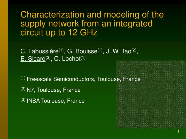
Characterization and modeling of the supply network from an integrated circuit up to 12 GHz. C. Labussière (1) , G. Bouisse (1) , J. W. Tao (2) , E. Sicard (3) , C. Lochot (1) (1) Freescale Semiconductors, Toulouse, France (2) N7, Toulouse, France (3) INSA Toulouse, France. Summary.

E N D
Characterization and modeling of the supply network from an integrated circuit up to 12 GHz C. Labussière(1), G. Bouisse(1), J. W. Tao(2), E. Sicard(3), C. Lochot(1) (1) Freescale Semiconductors, Toulouse, France (2) N7, Toulouse, France (3) INSA Toulouse, France
Summary • Context • Objectives • This work • Measurement approach • Experiments • Model validation • Conclusion
Equipment designers want to ensure EMC before fabrication Main source : micro-controller Context Courtesy C. Marot Siemens Automotive Toulouse
1. Context dBµV 16-bit micro-controller radiation in TEM cell, various programs 1 MHz 10 MHz 100 MHz 1 GHz
New bands of interest PowerPC 32 bits 80 60 40 20 0 1. Context Parasitic Emission (dBµV) • New concerns from 1 to 10 GHz 100 HC12 16 bit 1GHz 100 GHz 10MHz 100MHz 10GHz Frequency
1. Context • Pressure on IC vendors to provide parasitic emission models up to 5 GHz • Existing standards to modelize IC core, internal supply network, I/O interface and package • Models mostly valid up to 1 GHz Ibis ICEM
Measurements Frequency measurements Time-domain measure Fourier Transform This work 2. This work • Strategy to validate emission models for micro-controllers Simulations Core Model Package Model Probe Model Test board Model Analog Time Domain Simulation Fourier Transform Compare dBµV vs. frequency
2. This work • Characterize the Passive Distribution Network (PDN) of a 16-bit µc Freescale (S12X family, QFP 144 pins) • Build a specific board for high-precision measurements • Investigate the impedance behavior up to 12 GHz • Build a model based on R,L,C elements • Promote this approach as part of the eXtended-ICEM model initiative
Supply1 supply2 S ground RLC values tuned to fit with measurements Supply2 Supply1 Requi/2 Lequi/2 Requi/2 Lequi/2 Dut Cequi ground 3. Measurement approach Base on [s] parameter characterization (s11, s12) Vector Network Analyzer
3. Measurement approach Non-coaxial Measurements Issue measurement plane (short-open –load calibration) measurement plane DUT plane DUT plane b1 b’1 b’2 b2 a1 a’1 a’2 a2 to network analyzer port 2 to network analyzer port 1 DUT transition line [s] parameters of the DUT alone can be found by de-embedding using Thru-Reflect-Line (TRL method)
DUT plane meas. plane meas. plane DUT plane [S]lineA [S]DUT [S]lineB 3. Measurement approach Method (1/3) • Measurement of 3 calibration features with known [S] matrix Thru Reflect Line
DUT plane meas. plane meas. plane DUT plane [S]lineA [S]DUT [S]lineB 3. Measurement approach Method (2/3) • Measurement of 3 calibration features with known [S] matrix • Characterization of the transition lines [S] matrices [S]lineA [S]lineB
DUT plane meas. plane meas. plane DUT plane [S]-1lineA [S]lineA [S]DUT [S]lineB [S]-1lineB [S]DUT 3. Measurement approach Method (3/3) • Measurement of 3 calibration features with known [S] matrix • Characterization of the transition lines [S] matrices • Determination of the DUT [S] matrix by automatic de-embedding
High-frequency “Delay” type 1 Lines type 1 Lines type 2 High-frequency “Delay” type 2 “Thru” type 2 “Reflect” type 2 S12X SMA connectors “Reflect” type 1 “Thru” type 1 4. Experiments Test boards Access+DUT Calibration boards
V DDX1 VSSA VSSX1 VDDA VDD1 S12X SS2 VSS1 144 LQFP VDD2 VDDX2 VDDR2 VSSX2 VSSR2 VDDR1 VSSPLL VDDR1 VDDPLL 4. Experiments 8 pairs of VDD/VSS power and ground pins Test specification (1/2) Nearly 120 possible measurements Select the key measurements to build the passive distribution network model
4. Experiments Test specification (2/2) Logic core decoupling Analog supply IO supply Other IO supply Substrate coupling
0.05 Ω 0.05 Ω VDDX1 VDDX2 0.05 Ω 0.05 Ω VSSX2 VSSX1 0.15 Ω 0.2 Ω 0.1 Ω 0.1 Ω VDDR1 VDDR2 0.05 Ω 0.05 Ω VSSR2 VSSR1 0.05 Ω VDDA 0.05 Ω VSSA 25.9 Ω 1 Ω 0.9 Ω VDD1 VDD2 0.75 Ω 0.55 Ω VSS2 VSS1 VDDPLL 12 Ω VSSPLL 4. Experiments Measurement (1/2)
4. Experiments Measurement (2/2) VSS1-VSS2 [s12] up to 12 GHz Low impedance 1.8 GHz Substrate coupling (RDC=1.8 ohm) Inductive High impedance 900 MHz 5 GHz
5. Model Validation Manual fitting of magnitude and phase by iteration Simulation Measure Simulation Measure
5. Model Validation Partial model of the passive supply network including the inductive path and resistive coupling
5. Model Validation VSS1-VSS2 [s12] up to 12 GHz 1 GHz 5 GHz Possible susceptibility issues
[SVDD1-VDD2] [TVDD1-VDD2] = [Td1]*[Td2] [SVSS1-VSS2] [TVSS1-VSS2] = [Ts1]*[Ts2] [SVDD1-VSS1] [TVDD1-VSS1] = [Td1]*[Tc]*[Ts1] [SVDD2-VSS2] [TVDD2-VSS2] = [Td2]*[Tc]*[Ts2] [SVDD1-VSS2] [TVDD1-VSS2] = [Td1]*[Tc]*[Ts2] [Td1], [Td2], [Tc], [Ts1], [Ts2] [Sd1], [Sd2], [Sc], [Ss1], [Ss2] spice-compatible behavioral model 5. Model Validation Complete S12X supply network construction from 2-port [s] models VDD1 VDD2 T T d2 d1 T c VSS1 VSS2 T T s2 s1
Conclusion • A technique for integrate circuit supply network characterization has been presented • A specific board is required to characterize the impedance up to 12 GHz • The technique is adaptable to BGA packages • An impedance model has been derived, valid up to 12 GHz • Resonance effects (0.9, 5 GHz) may generate susceptibility issues

![What is an IC ? [integrated circuit]](https://cdn1.slideserve.com/2972450/slide1-dt.jpg)