Download
1 / 49
490 likes | 637 Views
5.6 Cache Coherency Issues. cache coherency problem: when the cache and main memory do not have the same data (stale data problem) stale data problem can appear in both uniprocessor (write back Fig. 5.22) and multiprocessor environment. 5.6.2 Software Solutions.

E N D
cache coherency problem: when the cache and main memory do not have the same data (stale data problem) • stale data problem can appear in both uniprocessor (write back Fig. 5.22) and multiprocessor environment
5.6.2 Software Solutions • rely on compiler to mark software code module and data structure as shared/noncacheable, exclusive (usually on a page basic) • shared page are never cached • shared but only for read-only operations, such as code of critical sections • shared pages marked as “exclusive”, that only available in this cache (only one processor can modify) and do write transition
5.6.3 Hardware Solutions • cacheabable/noncacheable memory: • main memory are designated as noncacheable (accesses to them are cache misses) and cacheable • Fig. 5.23a, external cache, Fig. 5.23b, internal cache, the external decoder will signal back the processor to bypass or disable the on-chip cache (i.e., do not update it with a value coming from a noncacheable location of main memory)
shared cache: • fig. 5.24 all bus masters are routed to main memory through the same cache
bus snooping (for multi bus master system): • Case 1: cache use write-back mode, I/O read stale data from main memory (stale data in memory) • cache controller monitor the memory/system bus for reads • if in the cache, it inhibits the I/O system from reading from memory and the cache controller itself provides the data from its cache to the I/O system • Case 2: cache with a write-through mode, I/O write to main memory (stale data in cache) • cache controller monitor the memory/system bus for write • if the target address is in the cache, then change the cache into invalidate, the next microprocessor read operation will read from main memory
EX: 5.8 Intel 80486 On Chip snooping hardware • The 80486 address bus is input/output, unlike the 80386 address bus, which is output only
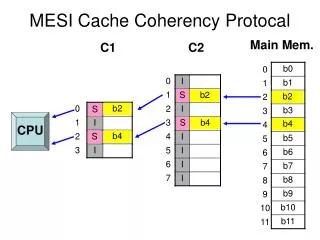
M.E.S.I. hardware cache coherency protocol • A hardware-implemented cache coherency protocol • Each cache line has 4-state which define whether a line is valid, if it is available in other caches (shared or exclusive), and if it is modified (has been modified) • Modified (M): indicate a line is available only in this cache and is modified (main memory’s copy is stale). • Can be updated locally in the cache without acquiring the memory bus • Exclusive (E): indicate a line is exclusively available only in this cache and is not modified (main memory also has a valid copy) • Write to exclusive line causes it to change to the modified state and don’t need to inform other caches (no memory bus acquiring) • Shared (S): indicate the line is shared with other caches (the line may exist in one or more other caches) • Can be read by the CPU without a main memory access • Writing to a shared line updates the cache and also requires to write through cycle to the memory bus (invalidate this line in other caches) • Invalid (I): indicate the line is not available in the cache • To read this cache line will be a miss and to execute a line fill • To write this cache line will only do the write to main memory
Basic State Transitions • the state determine the actions of the cache controller with regard to activity related to a line, and the state of a line may change due to those actions. • All transactions which may require state changes in other caches are broadcast on the shared memory bus. • For example, if a bus transaction requires that a line in another cache be invalidated, the memory bus controller is responsible for asserting an invalidation signal on the bus • The M.E.S.I. model describes a write-back cache. A write-through cache is a true subset of this model with only the shared and invalid states being implemented
Current state: refers to the state of the cache line being accessed by its CPU • Action state: refers either to a CPU “read” CPU “write,” or a “snoop” initiated by another cache attached to the same shared memory bus. • New state: refers to the state of the current cache line after the action is performed. • Memory bus activity: refers to the action which takes place on the memory bus (if any) as a result of the action being performed on the cache line.
Introduction to the MESI Model • In multi-processing environment where several cache subsystems exist • More than one cache may contain a copy of information form a given memory location • Need to maintain cache consistency • The MESI model • Every line in cache is assigned one of these 4-state • Transitions from one state to another may be caused by • A local processor read or write • A bus snoop when another bus master initiates bus activity
state diagram of MESI transitions that occur within the Pentium’s data cache
Pentium Processor System Architecture • The code cache only uses a subset of the MESI model • Because the code cache is a read-only cache • We only discuss the data cache • In the following, the operation of the L2 cache is a write-back cache • Implement back-off when detecting a snoop hit to a modified line • The interaction between the level 1 and level 2 caches is a write-once policy (depend on the L2 cache indication)
Pentium Cache Organization • initial reset: all cache line are invalid (I-state) • CPU accesses new data • cache miss, data will be retrieved from main memory and stored first in the L2 cache and then into the L1 data cache. • L1 state is shared (S-state, due to WB/WT# = 0), L2 state is exclusive (E-state) • CPU first writes to this line • write to L1 cache (update), because L1 is S-state, => write to L2 (update, L1, L2 consistency), L2 changed to M-state, L1 changes to E-state • A subsequent update to the line in L1 => L1 changes to M-state and all of the subsequent updates, there is no transfer to L2 • This is known as a write-once policy • because L1 in E-state or M-state means only CPU uses the data, but L2 in M-state => if snoop the data hit, L2 informs L1 to do write-back • Finally, when L1 is necessary to replace a line • if L1 is in the S or E state, it need not be written out. • If it is in the M state, the line is written back to the L2 cache and then flushed from the L1 cache.
L2 operation: • Firstly, read data into the L1 and L2 caches • the line in the L2 is E-state (L2 is the newest data, exclusive to the processor and L1 cache) • When a write-once occurs, the L2 updates the line and changes to M-state (for other bus master). • The L2 will not be notified of any subsequents updates to this line by the L1 cache. • L2 snoop another bus master read data stored in an L2 line that is in the M state, • L2 causes the bus master to back off and passes the requested address to the L1. L1 performs a write-back cycle to update main memory.
If another bus master attempts to write data that is in an L2 line in the M state, then blocks the action. • L2 cache detects and blocks the write operation • L2 signal the L1 with the address of the write operation. • If the L1 has been updated since the write-once (M-state), it performs a write back the modify data to main memory and change to I-sate • If L1 doesn’t do the write back, the L2 update the main memory and changes to I-state • L2 release the bus master, allowing it to complete the write operation
summary • Initial : • L1 = I-state, L2 = I-state • Initial access: • L1 and L2 cache miss, L1 and L2 cache update, L2: E-state and asserts WB/WT# = 0 to L1 for write-once policy => L1: S-state • First write: • L1 update and write through to L2, L1 state: S => E • L2 update and assert WB/WT=1 for L1, L2 state: E => M • Consequence write: • L1: update (write back not write through), state: E => M • L2: stale data, state: M => M
Single processor system • Case1: other bus master read from line stored in the L2 : M state, L1 = E state. • L2: snoops the address driven by the bus master (will receive stale data), • L2 backed off the bus master, L2 transfer the address to the CPU, because L2 in M state and doesn’t make sure the data is fresh data • L2 asserts AHOLD to CPU to float its address bus, and passes the read address driven by the another bus master. Next, L2 asserts the EADS signal to CPU for CPU snooping the address. • If L1 = E-state (the line has not been updated since it was last written through to the L2 cache), CPU asserts HIT# to L2 (means snoop hit on a clean line) • L2: deasserts INV (INV = 0) to L1 (mean the snooping is read cycle by another bus master), then L1 state: E => S. L2 sample the HIT# and HITM# deasserted, L2 knows that it has the latest information => L2 do write-back to system memory. L2 state: M => E (if only one cache in the system) otherwise M => S
Case 2: other bus master read from line stored in the L2 : M state, L1 = M state. • the L1 asserts the HIT# (mean the access data in the L1) and HITM# (the access data has been modified in L1) to L2 • L1 run a write-back to main memory and L2 do the update • L2 asserts INV = 0 (mean snoop read), L1: M => S, L2: M => E (single cache in the system) or M => S (if multiple cache in the system)
Case 3: other bus master write and the L2 : M state, L1 = E/M state. • HITM# value is depended on L1 state (E or M) • L2 assert INV = 1, • if L1: E-state => I state, L2 write back and M=> I • if L1: M-state, L1 write back, L1: M=> I, L2: M => I
Multiprocessor MESI Implementation • Read by processor B from a line present in processor A’s cache • Table 4-2 initial state of cache line for processor A’s cache • Scenario 1: L2: E, L1: S (after line-fill operation), same with L2:S, L1:S • Scenario 2: L2: M, L1: E (after 1st internal write to target line, L2 data is fresh) • Scenario 3: L2: M, L1: M (L2 data is stale)
Scenario 1 (The initial cache state) • Processor A has just completed a read from a memory location for the first time. L1: S-state (consistent with the write-once policy). L2: E-state • The read miss in the B complex: • B initiates the read, L1 miss and access is transferred to the L2. The L2 also results in a miss, followed by a bus cycle to system memory to perform a cache line-fill. • The Snoop By processor A: • Processor A’s L2 cache detects the read bus cycle and snoops the address. L2 in the E state, so it experiences a snoop hit. L2 change to the S-state. (because the other bus master will store the line in its cache). No inquire cycle need be sent to Pentium L1 cache, because L2 previous state is E-state (doesn’t modify) • The Read bus cycle completes: • When the hit is detected, the processor A L2 cache asserts its cache hit (CHIT#) signal to processor B that it is about to read data shared by another cache in the system (but doesn’t modify because CHITM# doesn’t asserted) => B’s L2 need store in S-state (if CHIT# doesn’t asserted, the L2 state is E-state), The L2 cache drives the WB/WT# signal low => B’s L1 store in S-state with write-through
Scenario Two: L1: E state , L2: M state • The initial cache state: after read a line from memory (L1: S-state, L2: E-state), the processor A updates the cache line in the L1 cache and write-through occurs because L1: s-state. => A’s L2 change to M-state, and L2 cache sets the WB/WT# line high, causing A’s L1 change to E-state (write-back, write-once)
Scenario Two: L1: E state , L2: M state (cont’d) • The cache read Miss in processor B: • B performs a read from a line, L1 miss (cause the processor to initiate a cache line-fill request on its external buses). The memory read also causes a miss in L2 and the bus cycle is transferred to the system bus for access to system memory. • The snoop by A: • A’s L2 detects the memory read bus cycle on the system bus and finds a copy of the target line in the M-state, the L2 determines that it must back off the other L2 cache. => A’s L2 asserts CHIT# and CHITM#, indicating a snoop hit to a modified line. • The backoff: • the CHIT# and CHITM# are inputs to the B’s L2 cache and direct it to backoff until the memory line has been updated by A => processor B L2 assert BOFF# (backoff) to force processor B to suspend the current bus cycle.
Scenario Two: L1: E state , L2: M state (cont’d) • Processor A’s L1 snoop: • A’s L2 determine if A’s L1 cache has more recent data than L2 does (L1: M-state) or not (L1: E state). • AHOLD is asserted by the L2 and it then passes the address to processor A. EADS# is asserted, telling the processor to snoop the address. INV is deasserted, indicating that the other bus master is performing a read, so there is no need to invalidate the L1 line in the event of a snoop hit. • L1 in the E-state: • The snoop results in a hit on a line in the E-state, indicating that it has not been modified. Processor a asserts HIT#, informing L2 that the inquire cycle resulted in a hit to a non-modified line. L1 state transitions from E to S.
Scenario Two: L1: E state , L2: M state (cont’d) • The write-back: • A’s L2 detects HIT# asserted => L2 has the most recent data. L2 performs a write-back cycle to fresh line in memory. L2 state updated from M to S. • BackOff removed and the read completes: • after the A’s L2 write-back, A’s L2 deasserts CHIT# and CHITM# => B’s L2 deasserts BOFF# to processor B. => processor B restarts the cache line-fill. B’s L2 in S-state and assert WB/WT# signal low. => B’s L1 in S-state with write-through operation.
Scenario Three: L1: M state, L2: M state • L1 write two times: S -> E -> M • L2 stale data: E -> M
Scenario Three: L1: M state, L2: M state (cont’d) • Processor B Read Cache Miss: • L1 miss, request L2 to line-fill => L2 miss, request system bus to do line-fill • The Snoop by Processor A: • detect processor B’s L2 cache do the line-fill request, processor A’s L2 experiences a snoop hit on a modified line. A’s L2 cache asserts CHITM# and CHIT# to B’s L2 cache. • Backoff of processor B: • the CHITM# instructs B’s L2 to abort the cache line-fill and B’s L2 asserts BOFF# to processor B, forcing the processor to about the cache line-fill request in progress on its local bus.
Scenario Three: L1: M state, L2: M state (cont’d) • The Inquire cycle to processor A: • A’s L2 inquire A’s L1 whether has more recent data than it does. • AHOLD is asserted and the memory read address generated by processor B’s L2 is passed to the processor A for snooping. EADS# is asserted to indicate processor A to snoop the address. • INV is deasserted, indicating that the cache line should remain valid in the event of a snoop hit (because B’s L2 is going to read, not modify it). • A’s L1 asserts HIT# and HITM# to inform the L2 that the inquire cycle resulted in a hit to a modified line
Scenario Three: L1: M state, L2: M state (cont’d) • Processor A performs the write-back: • the processor L1 will perform a write-back operation to deposit the fresh line in memory. L1 state M -> S • A’s L2 update its cache line and state: M -> S • Backoff removed from processor B and its cache-fill complete: • A’s L2 deasserts CHIT# and CHITM# (releasing B to restart the cache line-fill operation and fetch the fresh line from memory). • B’s L2 deasserts BOFF# to processor B. • B’s L2 reinitiated cache line-fill, A’s L2 snoop hit to a shared line. • A’s L2 asserts CHIT# but not CHITM#. => inform B’s L2 cache that another cache in the system has a copy of the target line currently being read from memory by B’s L2 cache. • B’s L2 : S-state, drive WB/WT# = 0, forcing B’s L1: S-state.
Multiprocessor MESI Implementation • Write by processor B to a Line presented in processor A’s cache
Scenario One : L1: S state, L2: E state • The initial cache state: A’s L1: S (WB/WT#=0), A’s L2 = E (L2 is fresh data)
Scenario One : L1: S state, L2: E state (cont’d) • Processor B experiences a double write miss: • B’s L1 miss, B’s L2 miss. B’s L2 asserts a memory write to system bus. • Processor A’s L2 cache snoops the memory write in progress: • A’s L2 snoop a write operation in a hit. A’s L2 state: E => I. • The inquire cycle to processor A: • A’s L2 asserts AHOLD and passes the address to the A’s local address bus. Once the address is stable, A’s L2 cache asserts EADS# and asserts INV. A’s L1 state: S => I, and A’s L1 asserts HIT# to A’s L2. A’s L2 no action is taken (don’t need to write back from L1 to L2). • Processor complex B completes the memory write bus cycle.
Scenario Two: L1: E state, L2: M state (cont’d) • Processor b’s double write miss: • L1 and L2 write miss, asserts a memory write bus cycle to update system memory • Processor A snoops the memory write: • A’s L2 snoops. A back off processor B and deposit the fresh line in memory before allowing B to finish the write transaction. • Processor A’s L2 cache back off processor B’s l2 cache: • A’s L2 asserts CHIT# and CHITM# => causes B to backoff. B’s L2 activates its BOFF# output forcing processor B to suspend the current bus cycle.
Scenario Two: L1: E state, L2: M state (cont’d) • Processor A snoops the address: • A’s L2 assert AHOLD to A’s L1. A’s L2 asserts EADS# and INV is asserted to A’s L1 => A’s L1 state: E => I. A’s L1 asserts HIT# (doesn’t assert HITM#). • Processor A’s L2 cache performs the write-back: • A’s L2 detects HIT# asserted, it knows that it has the most recent data. A’s L2 performs a write-back cycle to deposit the fresh line in memory so that it may be updated by the other bus master when the backoff is removed. A’s L2 state: M => I. • Backoff is removed by processor A’s L2 and processor B completes the memory update: • A’s L2 deasserts CHITM#, releasing processor B to reinitiate the write operation to update the line in memory. (B’s L2 deasserts BOFF# to processor B). when B restart memory write, A’s L2 snoops the address and detects a snoop miss.
Scenario three: L1: M state, L2: M state ,WB/WT# = 1 (cont’d) • Processor B experiences a double write miss. • Processor A snoops the memory write: • A’s L2 asserts CHIT# and CHITM# (because A’s L2 = M state) • The back off: • Processor A snoops the address: A’s L2 asserts AHOLD, EADS#, and INV to A’s L1. A’s L1 snoops hit and assert HIT# and HITM# to A’s L2. • Processor A’s L1 performs the write-back: A’s L1 perform write-back. A’s L2 state: M => I. A’s L1 state: M => I • Processor A’s L2 remove backoff and the processor B write is reinitiated.
Scenario four:The initial cache state: A’s L1: S, A’s L2: S. B’s L1: S, B’s L2: S • The write hit and write-through: • B experiences a write hit in its L1 cache. B update the line and do write-through. • B’s L2 also write hit. It updates the line and initiates a memory write bus cycle on the system bus. • B’s L2: S => E state, and asserts WB/WT# = 0 to instructs the B’s L1 to keep in the S state. • Processor A’s L2 snoops the memory write: • A detect the write on the system bus, and snoop hit to a shared line. A’s L2: S => I. Asserts AHOLD, EADS# and INV to A’s L1. A’s L1 asserts HIT# to A’s L2. A’s L1: S => I.