Download
1 / 8
80 likes | 308 Views
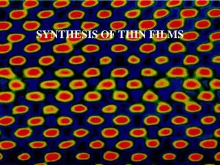
ECE 491 Meeting PVD Synthesis and electrical characterization of «?» thin films . Nov 24, 2011. MOTIVATION. To get a know «know how» to use PVD system in order to deposit a thin film To get experience on characterization techniques of thin films. OBJECTIVES.

E N D
ECE 491 MeetingPVD Synthesis and electrical characterization of «?» thin films Nov 24, 2011
MOTIVATION • To get a know «know how» to use PVD system in order to deposit a thin film • To get experience on characterization techniques of thin films
OBJECTIVES • Formation of «?» thin films by PVD • Electrical – Optical - Structural Caracterization of these thin films Therefore, the project is composed of TWO important parts: Synthesis Characterization
Methodology Determination of the starting parameters of PVD (P, T, t, substrate, target) Deposition of the Thin Film by PVD Electrical – Optical - Structural Characterization of these thin films Studying the effect of process parameters Optimization Simple Device Fabrication and tests
Questions to be answered • For which application? • Electrolumiscent device? • Sensor? • Which material will be deposited, what will be the source? • Which substrate will be used? • What are the parameters? What will be our starting parameters? • T, P, time, etc. • How does a PVD system operate? • What are electrical – optical – structural characterization techniques? selection of the characterization techniques and design of the set-ups for measurements. us you
TO DOGet an insight on: • Literature review on selected system • Vacuum Science and Technology (Chapter 2) • Gas Transport • Vacuum pumps and systems • Physical Vapor Deposition (Chapter 3) • Electrical Properties of Thin Films (Chapter 10) • Optical Properties of Thin Films (Chapter 11)
Semiconductor / Thin Film Characterization Techniques • What are the semiconductor quantities that could be characterized • depletion width, carrier concentration, optical generation and recombination rate, carrier lifetimes, defect concentration, trap states, etc. • These quantities fall into three categories when it comes to characterization methods: • Electrical Characterization • Optical Characterization • Structural/Physical/Chemical Characterization What are these quantities really?
Example1. Electrical Characterization Techniques • Used to determine which quantities, which property of material? • What are the different methods? • Principles of these methods? • Set-up? • Measures quantities? • Details....