Download
1 / 102
1.12k likes | 1.66k Views
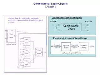
Combinatorial Logic Circuits. Index. Basic CMOS gates: Properties Ratioed Logic Pass transistor Logic Dynamic Logic. Out. In. Combinational. Combinational. In. Out. Logic. Logic. Circuit. Circuit. State. Combinational vs. Sequential Logic. Combinational. Sequential. Output =.

E N D
Index • Basic CMOS gates: Properties • Ratioed Logic • Pass transistor Logic • Dynamic Logic EE141
Out In Combinational Combinational In Out Logic Logic Circuit Circuit State Combinational vs. Sequential Logic Combinational Sequential Output = ( ) f In, Previous In Output = ( ) f In EE141
At every point in time (except during the switching transients) each gate output is connected to either V or V via a low-resistive path. DD ss The outputs of the gates assumeat all timesthevalue of the Boolean function, implemented by the circuit (ignoring, once again, the transient effects during switching periods). This is in contrast to the dynamic circuit class, which relies on temporary storage of signal values on the capacitance of high impedance circuit nodes. Static CMOS Circuit EE141
Static Complementary CMOS VDD F(In1,In2,…InN)=1 produce F=Vdd In1 In2 PUN … PMOS only InN F(In1,In2,…InN) In1 In2 PDN … NMOS only InN F(In1,In2,…InN)=0 produce F=GND PUN and PDN are dual logic networks EE141
NMOS Transistors in Series/Parallel Connection • Transistors can be thought as a switch controlled by its gate signal • NMOS switch closes when switch control input is high EE141
Example Gate: NAND EE141
Example Gate: NOR EE141
B A C D Complex CMOS Gate OUT = D + A • (B + C) A D B C EE141
V V DD DD C A SN4 F SN1 F B SN2 A A SN3 D D D B C B C F A (a) pull-down network (b) Deriving the pull-up network hierarchically by identifying D sub-nets B C (c) complete gate Constructing a Complex Gate EE141
Cell Design • Standard Cells • General purpose logic • Can be synthesized • Same height, varying width • Datapath Cells • For regular, structured designs (arithmetic) • Includes some wiring in the cell • Fixed height and width EE141
Standard Cell Layout Methodology – 1980s Routing channel VDD signals GND
Standard Cell Layout Methodology – 1990s Mirrored Cell No Routing channels VDD VDD M2 M3 GND Mirrored Cell GND
V DD Standard Cells N Well Cell height 12 metal tracks Metal track is approx. 3 + 3 Pitch = repetitive distance between objects Cell height is “12 pitch” Out In 2 Rails ~10 GND Cell boundary
V DD Standard Cells 2-input ??? gate A B Out GND
V V DD DD Stick Diagrams Contains no dimensions Represents relative positions of transistors Inverter NAND2 Out Out In A B GND GND
X PUN C i VDD X B A j PDN GND Stick Diagrams Logic Graph A j C B X = C • (A + B) C i A B A B C EE141
Two Versions of C • (A + B) A C B A B C VDD VDD X X GND GND Permutation of input signals that produce uninterrupted active strips is important !
Euler Paths • There is a systematic approach to uninterrupted strips of active. Two steps: • Step 1: Construction of logic graph • Step 2: Identification of Euler graphs • Euler path is a path through all nodes such that every edge is visited once. • Euler path is equivalent to an uninterrupted A-strip (succesive S and D connections) • Consistency: Same ordering for PUN and PDN EE141
Euler Path X Node C i VDD X B A j Edge = Transistor A B C GND EE141
OAI22 Logic Graph X PUN A C D C B D VDD X X = (A+B)•(C+D) C D B A A B PDN A GND B C D EE141
Example: x = ab+cd EE141
CMOS Gates • Static Properties of gates • Delay characteristics • Fan-in and Fan-out considerations EE141
3V a) A=B=0 → 1 Vout c) B=1, A=0 → 1 b) A=1, B=0 → 1 0V 3V 0V Vin Static Properties • Depend on input pattern • Two pull-up transistors in parallel are more difficult to turn off than one • One pull-up transistor, one pull-down. Dynamically, the internal node has to be discharged (slower) • Vds1 produces bulk effect during discharge. More Vin is needed EE141
Rp Rp Rp Rp Rp Rp A B A A B A Cint Rn CL CL CL Rn Rn Rn Rn B A A A B Cint Switch Delay Model Req A A NOR2 INV NAND2 EE141
Rp Rp B A Cint CL Rn A Input Pattern Effects on Delay • Delay is dependent on the pattern of inputs • Low to high transition • both inputs go low • delay is 0.69 Rp/2 CL • one input goes low • delay is 0.69 Rp CL • when N transistor A goes off, internal node has to be charged • High to low transition • both inputs go high • delay is 0.69 2Rn CL Rn B EE141
Delay Dependence on Input Patterns A=B=10 A=1 0, B=1 A=1, B=10 Voltage [V] time [ps] NMOS = 0.5m/0.25 m PMOS = 0.75m/0.25 m CL = 100 fF when N transistor A goes off, internal node has to be charged (slower) EE141
Rp Rp 2 2 Rp Rp B A A B Rn Cint Cint CL CL Rn Rn Rn B B A A 1 1 Transistor Sizing 4 4 2 2 NAND based implementations are preferred over NOR … EE141
A D Transistor Sizing a Complex CMOS Gate B 8 6 4 3 C 8 6 4 6 OUT = D + A • (B + C) A 2 D 1 B 2 C 2 EE141
D C B A C3 C2 C1 CL Fan-In Considerations Distributed RC model (Elmore delay) tpHL = 0.69 Re (C1+2C2+3C3+4CL) = Re C1+2 Re C2+3Re C3+4Re CL * Propagation delay deteriorates rapidly as a function of fan-in – quadratically in the worst case. (prop. to R×C) * Internal nodes important !! A B C D EE141
tp as a Function of Fan-In Intrinsec C increases linearly Series transistors cause a double slowdown Parallel transistors increase C quadratic tp (psec) tpHL tp tpLH linear fan-in Gates with a fan-in greater than 4 should be avoided. EE141
tp as a Function of Fan-Out All gates have the same drive current. tpNOR2 tpNAND2 tpINV tp (psec) Slope is a function of “driving strength” eff. fan-out EE141
tp as a Function of Fan-In and Fan-Out • Fan-in: quadratic due to increasing resistance and capacitance • Fan-out: each additional fan-out gate adds two gate capacitances to CL tp = a1FI + a2FI2 + a3FO EE141
C3 C2 C1 CL Fast Complex Gates: Design Technique 1 • Transistor sizing • as long as fan-out capacitance dominates • Progressive sizing Distributed RC line M1 > M2 > M3 > … > MN (the fet closest to the output is the smallest) Lower caps see smaller R InN MN In3 M3 In2 M2 In1 M1 Can reduce delay by more than 20%; decreasing gains as technology shrinks EE141
C2 C1 C1 C2 CL CL Fast Complex Gates: Design Technique 2 • Transistor ordering • Transistor with more activity or with latest changes on top critical path critical path 01 charged charged 1 In1 In3 M3 M3 1 1 In2 In2 M2 discharged M2 charged 1 In3 discharged In1 charged M1 M1 01 delay determined by time to discharge CL, C1 and C2 delay determined by time to discharge CL EE141
Fast Complex Gates: Design Technique 3 • Alternative logic structures F = ABCDEFGH There are techniques to minimize switching time: logical effort EE141
CL CL Fast Complex Gates: Design Technique 4 • Isolating fan-in from fan-out using buffer insertion EE141
Fast Complex Gates: Design Technique 5 • Reducing the voltage swing • linear reduction in delay (only when variation of Req is not substantial; after this, delay gets worse) • also reduces power consumption • But the following gate is much slower! • Or requires use of “sense amplifiers” on the receiving end to restore the signal level (memory design) tpHL= 0.69 (3/4 (CL VDD)/ IDSATn ) = 0.69 (3/4 (CL Vswing)/ IDSATn ) EE141
Stages with general logic • What happens in the general case: no longer inverters • Suppose we drive a load using a non-inverter stage • We increase the transistors by a factor g so that we have the same driving as the inverter (per input) • The input capacitance is g times bigger there’s more than one input tpo is the intrinsic time of a min. size inv. EE141
Logical Effort f – effective fanout p – intrinsic delay factor (multiple times of the inverter intrinsic delay) g – logical effort (ratio of its input capacitance to the inverter capacitance when sized to deliver the same current). Increases with gate complexity. Depends only on topology EE141
V V V DD DD DD A A B B 2 2 2 4 F F A 4 A 2 F A 1 A B 1 1 B 2 Inverter 2-input NAND 2-input NOR Logical Effort Logical effort quantifies how much less driving strength a gate has compared to an inveter g = 5/3 g = 4/3 g = 1 EE141
Intrinsic delay factors EE141
Logical Effort of Gates t pNAND g = 4/3 p = 2 d = (4/3)h+2 t pINV Normalized delay (d) g = 1 p = 1 d = h+1 F(Fan-in) 1 2 3 4 5 6 7 Fan-out (h) EE141
Logical Effort of Gates 2-input NAND: p=2; g=4/3 Inverter: P=1; g=1 5 4 3 Effort Delay 2 Normalized Delay 1 Intrinsic Delay 1 2 3 4 5 Fanout f EE141
Multistage Networks Stage effort: hi = gifi Path electrical effort: F = Cout/Cin Path logical effort: G = g1g2…gN Branching effort: B = b1b2…bN Path effort: H = GFB Path delay EE141
Add Branching Effort Branching effort: EE141
Optimum Effort per Stage When each stage bears the same effort: Stage efforts: g1f1 = g2f2 = … = gNfN Effective fanout of each stage: EE141
Sizing • After the fi’s have been obtained, the sizing factors si’s are calculated starting from the first one: • The others are obtained iteratively Reference: Sutherland, Sproull, Harris, “Logical Effort, Morgan-Kaufmann 1999. EE141