Download
1 / 28
280 likes | 466 Views
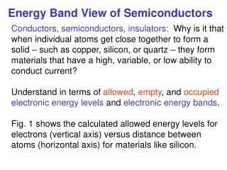
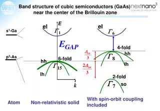
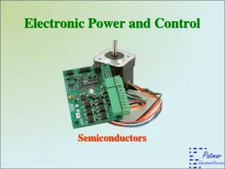
Semiconductors: Some theory and application. By: Bob Buckley. E. Let’s continue where we left off in class. Only partly filled electronic band can contribute to conductivity: Where does this partially filled band come from for semiconductors?. conduction band. E C. E g. E F. E V.

E N D
Semiconductors:Some theory and application By: Bob Buckley
E Let’s continue where we left off in class Only partly filled electronic band can contribute to conductivity: Where does this partially filled band come from for semiconductors? conduction band EC Eg EF EV valence band core electrons Semiconductor Insulator Metal
What is the requirement for electrical conduction in a solid? Conduction occurs when an electronic band is partially filled. Why? Due to the symmetry of a full band structure, for every electron with wavevector K, the band also contains an electron with wavevector –K. With a filled band, there is no way to continuously change the momentum of any of the electrons. This means they cannot change their motion. Of course a band that is empty of electrons cannot carry current. So, how does a semiconductor do it?
E kx k Remember Density of States: Free electron parabola What about for a semiconductor?
Density of electrons in conduction band: Density of holes in valence band: So what do the actual concentrations look like? As before, Density: We care about partially filled bands with respect to electrical conductivity.
Typically:: Eg>>kTRoom What does this mean for the concentrations, n and p First of all, since Eg>>kT, the Boltzmann approximation for the Fermi distribution is good for the allowed energies. For Eg>>kT
So, using the Boltzmann approximation: Substituting and
Let’s try something: What is n*p Notice: This result no longer depends on the Fermi energy For an intrinsic semiconductor, n=p for charge balance
How is the Fermi energy calculated for an intrinsic semiconductor: With some algebra:
E k Effective Mass Electrons in crystal are bound by the crystal and do not act like free electrons. Effective mass depends on the curvature of E(k) Remember: The more the curvature of E(k), the lighter the effective mass. For free electron:
E What about this k Properties of holes: • Kh = -Ke :: The wavevector of a hole is opposite to the wave vector of an e-The hole wavevector is the absence of the electron wavevector • Eh(Kh) = - Ee(Ke) :: Assuming zero energy at band gap Conduction band is concave up and valence band is concave down • Vh = Ve • mh = -me :: Curvature of e- valence band near top of curve is negative meaning hole mass near the top is positive
From table (and since Eg>>kT), it is evident that the concentrations of holes and conduction electrons are very small (ni) Compared to approx. 1023 atoms/cm^3 For example, actual resistivity of undoped GaAs is greater than 1E7 ohm-cm, this includes the effects due to defects such as unintentional doping Where μn and μp are the mobilities of the electrons and holes respectively Conductivity: What can we do to increase n and p in order to increase conductivity?
Semiconductor doping By increasing the concentration of either the conduction electrons or the holes in the valence band, we can increase the conductivity. This is done by substituting atoms in the semiconductor lattice that do not have four valence electrons, typically a valence 3 or 5 atom. N doping: A valence 5 atom contains one more electron than the intrinsic semiconductor. This extra electron, when excited goes into the conduction band. P doping: A valence 3 atom contains one less electron: (Or valence 4 plus one hole). When this hole is excited, it goes into the valence band. How exactly does this affect the semiconductor as a whole?
Picture a hydrogen atom superimposed inside a semiconductor lattice For H atom in free space: The semiconductor “background” must be accounted for: and Example, For Si: Bound e- is smeared over approximately 10^3 lattice sites
So, for a doped material, it takes a relatively small amount of energy to excite the extra electron (or hole) into the conduction band (valence band) of the material Remember np=constant for a specific type of semiconductor. Our assumptions of np still hold even with doped semiconductors Total charge is also conserved: Total concentration of doped atoms = Non-ionized atoms + ionized atoms: Typically, ND>>ni>p, so: Process is basically the same for a p doped semiconductor
It turns out statistically that the density of non-ionized dopant is the following: For n: For low enough temperatures: For high enough temperatures:
Carrier concentration vs. 1/T Conductivity vs. T Conductivity vs. 1/T
p n All of this theory can be interesting, but we all know semiconductors are crucial to electronic devices today Let’s look at a practical application: The p-n junction What is a p-n junction: A single crystal in which there is an abrupt change from a n-type to a p-type semiconductor
What happens when we have a joined p-n semiconductor? First of all, the electrochemical potential (EF) must be constant throughout the entire crystal for equilibrium In a p semiconductor, EF lies near the valence band. (It is lowered because of the decrease in electron density of the semiconductor) In a n semiconductor, EF lies near the conduction band. (The more number of electrons, the greater the largest energy at ground state) Since EFn=EFp, EV and EC are each shifted between the p and n regions This shift of both EV and EC creates a “band bending” This band bending is created by a macropotential which lies in the transition region This occurs because conduction electrons near the transition in the n region diffuse to the p region. Holes go the opposite way. The macropotential is created by static dopant ions when their electrons or holes diffuse into the part of the semiconductor doped oppositely
Differential Maxwell Equation for Gauss’ Law Due to symmetry, V and ρ only depend on one dimension Due to EV and EC shift and the resulting macropotential, we can say: And using previous equations for n, p, and np, We can say: Where pp is the density of holes in the pp region and nn is the density of conduction electrons in the n region, AKA majority carriers
V(x) n E(x) p -xp =-eVD xn =Constant ρ(x) + x x x - Static charges are due to ionized doping atoms.
Two types of charge motion are occurring simultaneously when this system is in equilibrium 1. Due to the holes’ and conduction electrons’ mobility and the fact that there is a concentration gradient at the junction, electrons diffuse from the n region to the p region while holes diffuse from the p region to the n region 2. Due to the macropotential voltage at the junction, electrons are pulled from the p region into the n region while holes are pulled from the n region into the p region. Due to the fact that there is no net current, jdiff=jdrift For electrons: For holes:
n p -xp xn ρ(x) + x - Is Einstein’s relation between D and µ Using Poisson equation, one can derive: Also:
n p -xp xn U - + ρ(x) p n + x - Let’s look at the non-steady state by applying a voltage across the junction: The width of the static charge region and the magnitude of VD are voltage dependent.
2 types of current: Originates when an electron in the p region or hole in the n region comes near the junction. This is quite “rare” since these are both minority carriers. Requires a thermal excitation. Jdrift or Igen This is basically independent of VD and therefore U since a thermal excitation must start the process. Remember Eg>>kT Jdiffusion or Irec Originates when an electron in the n region or hole in the p region is able to diffuse against (across) the potential barrier between the n and p regions. Majority carriers: Depends strongly on temperature because of the change in V
U - + p n By definition of Igen and Irec, positive current means majority carriers are moving to minority carriers Current is highly asymmetric Forward bias Reverse bias
Forward bias I Reverse bias U Semiconductor breakdown