Download
1 / 42
490 likes | 1.06k Views
Chapter 8 8051 Hardware Connection and Intel Hex File. Objective. 這章節要去了解8051每個角位的意義與用法 。 另外也要了解 Intel Hex File 的規格 。. Sections. 8.1 Pin description of the 8051 8. 2 Design and test of DS89C4x0 timer 8.3 Explaining the Intel hex file. Section 8.1 Pin Description of the 8051.

E N D
Objective • 這章節要去了解8051每個角位的意義與用法。 • 另外也要了解Intel Hex File的規格。
Sections 8.1 Pin description of the 8051 8.2 Design and test of DS89C4x0 timer 8.3 Explaining the Intel hex file
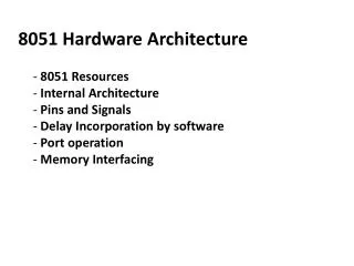
Packing Types of 8051 • The 8051 family members come in different packages, such as DIP(Dual In-line Package),QFP(Quad Flat Package)and LCC(Leadless Chip Carrier). • See Appendix H(Pages 621-623) • PDIP(Plastic DIP)& CERDIP(Ceramic DIP) • They all have 40 pins. • Figure 8-1. 8051 Pin Diagram • Also for 8052, 8031, DS89C4x0, AT89C51
Vcc P1.0 1 40 P0.0(AD0) P1.1 2 39 P0.1(AD1) P1.2 3 38 P0.2(AD2) P1.3 4 37 8051 P0.3(AD3) P1.4 5 36 P0.4(AD4) P1.5 6 35 P0.5(AD5) P1.6 7 34 P0.6(AD6) P1.7 8 33 P0.7(AD7) RST 9 32 (RXD)P3.0 EA/VPP 10 31 (TXD)P3.1 ALE/PROG 11 30 PSEN (INT0)P3.2 12 29 P2.7(A15) (INT1)P3.3 13 28 (T0)P3.4 P2.6(A14) 14 27 (T1)P3.5 P2.5(A13) 15 26 P2.4(A12) (WR)P3.6 16 25 P2.3(A11) (RD)P3.7 17 24 P2.2(A10) XTAL2 18 23 P2.1(A9) XTAL1 19 22 P2.0(A8) GND 20 21 PDIP/CERDIP Figure 8-1. 8051 Pin Diagram
Pins of 8051(1/5) • Vcc(pin 40): • Vcc provides supply voltage to the chip. • The voltage source is +5V. • GND(pin 20):ground • XTAL1 and XTAL2(pins 19,18): • These 2 pins provide external clock. • Way 1:using a quartz crystal oscillator • Way 2:using a TTL oscillator • Example 8-1 shows the relationship between XTAL and the machine cycle.
Pins of 8051(2/5) • I/O port pins • The four ports P0, P1, P2, and P3. • Each port uses 8 pins. • All I/O pins are bi-directional.
Pins of 8051(3/5) • RST(pin 9):reset • It is an input pin and is active high(normally low). • The high pulse must be high at least 2 machine cycles. • It is a power-on reset. • Upon applying a high pulse to RST, the microcontroller will reset and all values in registers will be lost. • Reset values of some 8051 registers • Way 1:Power-on reset circuit • Way 2:Power-on reset with debounce
Pins of 8051(4/5) • /EA(pin 31):external access • There is no on-chip ROM in 8031 and 8032 . • “/” means active low. • The /EA pin is connected to GND to indicate the code is stored externally. • For 8051, /EA pin is connected to Vcc. • /PSEN & ALE are used for external ROM too. • /PSEN(pin 29):program store enable • This is an output pin and is connected to the OE pin of the ROM. • See Chapter 14.
Pins of 8051(5/5) • ALE(pin 30):address latch enable • 8051 port 0 provides both address and data. • The ALE pin is used for de-multiplexing the address and data by connecting to the G pin of the 74LS373 latch. • It is an output pin and is active high. • When ALE=1, P0 provides address A0-A7. • When ALE=0, P0 provides data D0-D7.
Using a quartz crystal oscillator We can observe the frequency on the XTAL2 pin. C2 XTAL2 ) | 30pF C1 ) | XTAL1 30pF GND Figure 8-2 (a). XTAL Connection to 8051
Using a TTL oscillator XTAL2 is unconnected. XTAL2 NC EXTERNAL OSCILLATOR SIGNAL XTAL1 GND Figure 8-2 (b). XTAL Connection to an External Clock Source
Example 8-1 Find the machine cycle (MC) for the following chip if XTAL = 11.0592 MHz (a) AT89C51 (b) DS89C4x0 (c) DS5000 Solution: 1/11.0592 MHz = 90.42 ns (a) 1 MC = 90.42 ns 12 = 1.085 s (b) 1 MC = 90.42 ns 1 = 90.42 ns (c) 1 MC = 90.42 ns 4 = 361.68 ns
Port 0(pins 32-39) • P0 is an open drain. • Open drain is a term used for MOS chips in the same way that open collector is used for TTL chips. • When P0 is used for simple data I/O, we must connect it to external pull-up resistors. • Each pin of P0 must be connected externally to a 10K ohm pull-up resistor. • With external pull-up resistors connected upon reset, port 0 is configured as an output port. • When P0 is used for address/data multiplexing, it is connected to the 74LS373 to latch the address.
Vcc 10 K Port 0 P0.0 P0.1 DS5000 8751 8951 P0.2 P0.3 P0.4 P0.5 P0.6 P0.7 Figure 8-4. Port 0 with Pull-Up Resistors
Port 1(pins 1-8) • Port 1 does not need any pull-up resistors since it already has pull-up resistors internally. • Usually used for I/O.
Port 2(pins 21-28) • Port 2 does not need any pull-up resistors since it already has pull-up resistors internally. • In an 8031-based system, P2 are used to provide address A8-A15.
Port 3(pins 10-17) • Port 3 does not need any pull-up resistors since it already has pull-up resistors internally. • Port 3 has the additional function of providing signals. • Serial communications signal:RxD, TxD(Chapter 10) • External interrupt:/INT0, /INT1(Chapter 11) • Timer/counter:T0, T1(Chapter 9) • External memory accesses in 8031-based system:/WR, /RD(Chapter 14)
P3 Bit Function Pin P3.0 RxD 10 P3.1 TxD 11 P3.2 INT0 12 P3.3 INT1 13 P3.4 T0 14 P3.5 T1 15 P3.6 WR 16 P3.7 RD 17 Table 8-1: Port 3 Alternate Functions
Table 8-2: RESET Value of Some 8051 Registers Register Reset Value PC 0000 ACC 0000 B 0000 PSW 0000 SP 0007 DPTR 0000 RAM are all zero.
Vcc + ) | 10 uF 31 ) | EA/VPP X1 30 pF 19 11.0592 MHz 8.2 K ) | X2 18 30 pF RST 9 Figure 8-3 (a). Power-On RESET Circuit RST /EA
Figure 8-3 (b). Power-On RESET with Debounce Vcc 31 EA/VPP ) | X1 10 uF 30 pF X2 ) | RST 9 8.2 K
PSEN OE ALE 74LS373 CE G P0.0 P0.7 A0 A7 D D0 D7 EA P2.0 P2.7 A8 A15 8051 ROM Page 422 /OE: output Enable /CE: chip enable Figure 14-11 74LS373 Page 426 Fig14-8 G: Enable /PSEN ALE: next page
PSEN OE ALE 74LS373 CE G P0.0 P0.7 A0 A7 D D0 D7 EA P2.0 P2.7 A8 A15 8051 ROM Reading ROM (1/2) 2. 74373 latches the address and send to ROM 1. Send address to ROM High Address
PSEN OE ALE 74LS373 CE G P0.0 P0.7 A0 A7 D D0 D7 EA P2.0 P2.7 A8 A15 8051 ROM Reading ROM (2/2) 2. 74373 latches the address and send to ROM Low Address 3. ROM send the instruction back ALE
Figure 8-6. DS89C4x0 Trainer (for MAX232 connection, see Section 10.2)
Figure 8-7. Screen Capture from HyperTerminal for DS89C4x0 Trainer
Table 8-3. Clocks per Machine Cycle (MC) for Various 8051 Versions
Table 8-4. On-Chip Flash ROM Size for the DS89C4x0 Family from Maxim-Dallas Semiconductor. See www.maxim-ic.com
Intel Hex File • Intel hex file is a file format designed to standardize the loading of executable machine code. • Loaders in every ROM burners support Intel hex file format. • The loader use the Intel hex file to download the opcode into ROM. • In DOS-based PC, you need a utility called OH (object-to-hex) to produce Intel hex file format. • The process of writing a 8051 program *.asm *.obj *.abs Intel hex file ROM editor assembler linker OH loader
Syntax in Figure 8-9. • “:” Each line starts with a colom • CC is the count of byte in this line. • CC can range from 00 to 10H • AAAA is for the 16-bit address. • TT is for type. • TT=00 : more line to come after this line • TT=01 : last line. • D is data (or code). • SS is a single byte of checksum. See Example 8-4
Example 8-3 From Figure 8-9, analyze the six parts of line 3. Solution: :07 0020 00 DBFEDCFADDF62235 07: seven bytes of data 0020: the address of first byte in this line 00: not last line DB FE DC FA DD F6 22: data (lines 17-20) 35: checksum
Example 8-4 (a) Verify the checksum byte for line 3 of Figure 8-9. (b) Verify also the information is not corrupted. Solution: :07 0020 00 DBFEDCFADDF62235 (a) The sum is =07+00+20+00+DB+FE+DC+FA+DD+F6+22=5CBH The carry is dropped and checksum=100H-CBH=35H (b) Verify the information 07+00+20+00+DB+FE+DC+FA+DD+F6+22+35H =600H The carry is dropped and the result = 00H
Example 8-5 Compare the data portion of the Intel hex file of Figure 8-9 with the opcodes in the list file of the test program given in Figure 8-8. Do they match? Solution: In the first line of Figure 8-9, the data portion starts with 75H, the opcode for the instruction “MOV”, as shown in the list file of Figure 8-8. The last byte of the data in line3 of Figure 8-9 is 22, which is the opcode for the “RET” in the list file of Figure 8-8.
You are able to (1/2) • Explain the purpose of each pin of the 8051 microcontroller • Show the hardware connection of the 8051 chip • Explain how to design an 8051-based system • Show the design of the DS89C4x0 Trainer • Code the test program in Assembly and C for testing the DS89C4x0 • Show how to delete programs for DS89C4x0 flash ROM using PC HyperTerminal
You are able to (2/2) • Show how to download programs into a DS89C4x0 system using PC HyperTerminal • Explain the Intel hex file