Download
1 / 38
410 likes | 457 Views
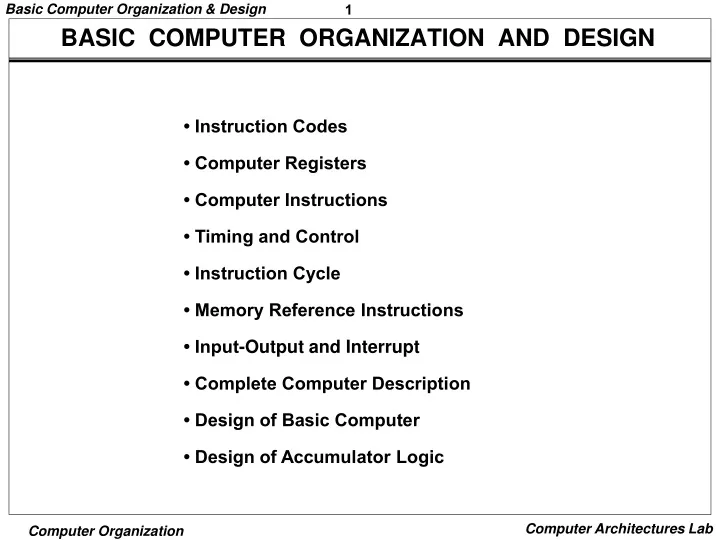
BASIC COMPUTER ORGANIZATION AND DESIGN. • Instruction Codes • Computer Registers • Computer Instructions • Timing and Control • Instruction Cycle • Memory Reference Instructions • Input-Output and Interrupt • Complete Computer Description • Design of Basic Computer

E N D
BASIC COMPUTER ORGANIZATION AND DESIGN • Instruction Codes • Computer Registers • Computer Instructions • Timing and Control • Instruction Cycle • Memory Reference Instructions • Input-Output and Interrupt • Complete Computer Description • Design of Basic Computer • Design of Accumulator Logic
Instruction codes INSTRUCTION CODES • Program: A set of instructions that specify the operations, operands, and the sequence by which processing has to occur. • Instruction Code: A group of bits that tell the computer to perform a specific operation (a sequence of micro-operation) -->macro-operation - usually divided into operation code, operand address, addressing mode, etc. - basic addressing modes Immediate, Direct, Indirect • Simplest stored program organization Memory 4096x16 15 12 11 0 Opcode Address Instructions Instruction Format (program) 15 0 Operands Binary Operand (data) Processor register (Accumulator, AC)
Mano's Basic Computer • Memory unit with 4096 l6-bit words • Registers: AR, PC, DR, AC, IR, TR, OUTR, INPR, SC • Flip-flops: t. S, E, R, fEN, FGI, FGO • 3 x 8 op decoder and 4 x 16 timing decoder • 16-bit common bus • Control logic gates • Adder and logic circuit connected to input of AC
Instruction codes INDIRECT ADDRESS Instruction Format 15 14 12 11 0 Opcode Address I Indirect address Direct Address 0 ADD 1 ADD 457 35 300 22 1350 300 Operand 457 1350 Operand + + AC AC Effective Address(EFA, EA) The address, that can be directly used without modification to access an operand for a computation-type instruction, or as the target address for a branch-type instruction
Registers COMPUTER REGISTERS Registers in the Basic Computer 11 0 PC 11 0 Memory AR 4096 x 16 15 0 IR 15 0 15 0 TR DR 7 0 7 0 15 0 OUTR INPR AC List of BC Registers • DR 16 Data Register Holds memory operand • AR 12 Address Register Holds address for memory • AC 16 Accumulator Processor register • IR 16 Instruction Register Holds instruction code • PC 12 Program Counter Holds address of instruction • TR 16 Temporary Register Holds temporary data • INPR 8 Input Register Holds input character • OUTR 8 Output Register Holds output character
Program Counter (PC) • Holds memory address of next instruction It • Next instruction is fetched after current instruction completes execution cycle It 0 • PC is incremented right after instruction is fetched from memory 15 0 16 bits per word • PC value can be replaced by new address when executing a branch instruction
Register Control Inputs • Load (LD) • Increment (INR) • Clear (CLR)
Common Bus • Connects registers and memory • Specific output selected by S2SISO • When register has < 16 bits, high-order bus bits are set to 0 • Register with LD enabled reads data from bus • Memory with Write enabled reads bus • Memory with Read enabled puts data on bus • When S2SlS0 = III
Address Register (AR) • Always used to specify address within memory unit • Dedicated register eliminates need for separate address bus • Content of any register output connected to the bus can be written to memory • Any register input connected to bus can be target of memory read • As long as its LD is enabled
Accumulator (AC) • Input comes from adder and logic circuit • Adder and logic circuit • Input • 16-bit output of AC • 16-bit data register (DR) • 8-bit input register (INPR) • Output • 16-bit input of AC • E flip-flop (extended AC bit. aka overflow) • DR and AC input used for arithmetic and logic microoperations
Registers COMMON BUS SYSTEM S2 S1 Bus S0 Memory unit 7 4096 x 16 Address Write Read AR 1 LD INR CLR PC 2 LD INR CLR DR 3 LD INR CLR E Adder and logic AC 4 LD INR CLR INPR IR 5 LD TR 6 LD INR CLR OUTR Clock LD 16-bit common bus
Instructions 15 12 11 0 Register operation 0 1 1 1 15 12 11 0 I/O operation 1 1 1 1 COMPUTER(BC) INSTRUCTIONS Basic Computer Instruction code format Memory-Reference Instructions (OP-code = 000 ~ 110) 15 14 12 11 0 Opcode Address I Register-Reference Instructions (OP-code = 111, I = 0) Input-Output Instructions (OP-code =111, I = 1)
Instructions BASIC COMPUTER INSTRUCTIONS Hex Code Symbol I = 0 I = 1 Description • AND 0xxx 8xxx AND memory word to AC • ADD 1xxx 9xxx Add memory word to AC • LDA 2xxx Axxx Load AC from memory • STA 3xxx Bxxx Store content of AC into memory • BUN 4xxx Cxxx Branch unconditionally • BSA 5xxx Dxxx Branch and save return address • ISZ 6xxx Exxx Increment and skip if zero • CLA 7800 Clear AC • CLE 7400 Clear E • CMA 7200 Complement AC • CME 7100 Complement E • CIR 7080 Circulate right AC and E • CIL 7040 Circulate left AC and E • INC 7020 Increment AC • SPA 7010 Skip next instr. if AC is positive • SNA 7008 Skip next instr. if AC is negative • SZA 7004 Skip next instr. if AC is zero • SZE 7002 Skip next instr. if E is zero • HLT 7001 Halt computer • INP F800 Input character to AC • OUT F400 Output character from AC • SKI F200 Skip on input flag • SKO F100 Skip on output flag • ION F080 Interrupt on • IOF F040 Interrupt off
Instructions INSTRUCTION SET COMPLETENESS A computer should have a set of instructions so that the user can construct machine language programs to evaluate any function that is known to be computable. Instruction Types • Functional Instructions • - Arithmetic, logic, and shift instructions • - ADD, CMA, INC, CIR, CIL, AND, CLA • Transfer Instructions • - Data transfers between the main memory • and the processor registers • - LDA, STA • Control Instructions • - Program sequencing and control • - BUN, BSA, ISZ • Input/Output Instructions • - Input and output • - INP, OUT
Timing and control TIMING AND CONTROL Control unit of basic computer Instruction register (IR) 14 13 12 15 11 - 0 Other inputs 3 x 8 decoder 7 6 5 4 3 2 1 0 D 0 I Control D Control outputs 7 logic gates T 15 T 0 15 14 . . . . 2 1 0 4 x 16 decoder Increment (INR) 4-bit sequence Clear (CLR) counter Clock (SC) Control unit implementation Hardwired Implementation Microprogrammed Implementation
Instruction Cycle INSTRUCTION CYCLE •Fetch instruction from memory • Decode the instruction • Read effective address from memory if indirect address • Execute the instruction Common bus
Fetch And Decode • se cleared to 0, generating timing signal To • After each clock pulse, se is incremented • Fetch and decode microoperations
Instrction Cycle DETERMINE THE TYPE OF INSTRUCTION Start SC 0 T0 AR PC T1 IR M[AR], PC PC + 1 T2 Decode Opcode in IR(12-14), AR IR(0-11), I IR(15) (Register or I/O) = 1 = 0 (Memory-reference) D7 = 0 (direct) (I/O) = 1 = 0 (register) (indirect) = 1 I I T3 T3 T3 T3 Nothing Execute Execute AR M[AR] input-output register-reference instruction instruction SC 0 SC 0 Execute T4 memory-reference instruction SC 0 D'7IT3: AR M[AR] D'7I'T3: Nothing D7I'T3: Execute a register-reference instr. D7IT3: Execute an input-output instr.
Instruction Cycle REGISTER REFERENCE INSTRUCTIONS Register Reference Instructions are identified when - D7 = 1, I = 0 - Register Ref. Instr. is specified in b0 ~ b11 of IR - Execution starts with timing signal T3 r = D7 I’ T3 => Register Reference Instruction Bi = IR(i) , i=0,1,2,...,11 r: SC 0 CLA rB11: AC 0 CLE rB10: E 0 CMA rB9: AC AC’ CME rB8: E E’ CIR rB7: AC shr AC, AC(15) E, E AC(0) CIL rB6: AC shl AC, AC(0) E, E AC(15) INC rB5: AC AC + 1 SPA rB4: if (AC(15) = 0) then (PC PC+1) SNA rB3: if (AC(15) = 1) then (PC PC+1) SZA rB2: if (AC = 0) then (PC PC+1) SZE rB1: if (E = 0) then (PC PC+1) HLT rB0: S 0 (S is a start-stop flip-flop)
MR Instructions MEMORY REFERENCE INSTRUCTIONS Operation Decoder Symbol Symbolic Description AND D0 AC AC M[AR] ADD D1 AC AC + M[AR], E Cout LDA D2 AC M[AR] STA D3 M[AR] AC BUN D4 PC AR BSA D5 M[AR] PC, PC AR + 1 ISZ D6 M[AR] M[AR] + 1, if M[AR] + 1 = 0 then PC PC+1 - The effective address of the instruction is in AR and was placed there during timing signal T2 when I = 0, or during timing signal T3 when I = 1 - Memory cycle is assumed to be short enough to complete in a CPU cycle - The execution of MR Instruction starts with T4 AND to AC D0T4: DR M[AR] Read operand D0T5: AC AC DR, SC 0 AND with AC ADD to AC D1T4: DR M[AR] Read operand D1T5: AC AC + DR, E Cout, SC 0 Add to AC and store carry in E
MEMORY REFERENCE INSTRUCTIONS LDA: Load to AC D2T4: DR M[AR] D2T5: AC DR, SC 0 STA: Store AC D3T4: M[AR] AC, SC 0 BUN: Branch Unconditionally D4T4: PC AR, SC 0 BSA: Branch and Save Return Address M[AR] PC, PC AR + 1 Memory, PC, AR at time T4 Memory, PC after execution 20 0 BSA 135 20 0 BSA 135 PC = 21 Next instruction 21 Next instruction AR = 135 135 21 136 Subroutine Subroutine PC = 136 1 BUN 135 1 BUN 135 Memory Memory
MR Instructions MEMORY REFERENCE INSTRUCTIONS BSA: D5T4: M[AR] PC, AR AR + 1 D5T5: PC AR, SC 0 ISZ: Increment and Skip-if-Zero D6T4: DR M[AR] D6T5: DR DR + 1 D6T4: M[AR] DR, if (DR = 0) then (PC PC + 1), SC 0
MR Instructions FLOWCHART FOR MEMORY REFERENCE INSTRUCTIONS Memory-reference instruction AND ADD LDA STA D T D T D T D T 4 1 4 2 4 3 4 0 M[AR] <- AC DR <- M[AR] DR <- M[AR] DR <- M[AR] SC <- 0 D T D T D T 0 5 1 5 2 5 AC <- AC DR AC <- DR AC <- AC + DR SC <- 0 SC <- 0 E <- Cout SC <- 0 BUN BSA ISZ D T D T D T 4 4 5 4 6 4 PC <- AR M[AR] <- PC DR <- M[AR] SC <- 0 AR <- AR + 1 D T D T 5 5 6 5 PC <- AR DR <- DR + 1 SC <- 0 D T 6 6 M[AR] <- DR If (DR = 0) then (PC <- PC + 1) SC <- 0
I/O and Interrupt INPUT-OUTPUT AND INTERRUPT A Terminal with a keyboard and a Printer • Input-Output Configuration Serial registers and Input-output communication Computer terminal interface flip-flops Receiver Printer OUTR FGO interface AC Transmitter Keyboard INPR FGI interface INPR Input register - 8 bits OUTR Output register - 8 bits FGI Input flag - 1 bit FGO Output flag - 1 bit IEN Interrupt enable - 1 bit Serial Communications Path Parallel Communications Path - The terminal sends and receives serial information - The serial info. from the keyboard is shifted into INPR - The serial info. for the printer is stored in the OUTR - INPR and OUTR communicate with the terminal serially and with the AC in parallel. - The flags are needed to synchronize the timing difference between I/O device and the computer
I/O and Interrupt PROGRAM CONTROLLED DATA TRANSFER -- CPU -- -- I/O Device -- /* Input */ /* Initially FGI = 0 */ loop: If FGI = 0 goto loop AC INPR, FGI 0 /* Output */ /* Initially FGO = 1 */ loop: If FGO = 0 goto loop OUTR AC, FGO 0 loop: If FGI = 1 goto loop INPR new data, FGI 1 loop: If FGO = 1 goto loop consume OUTR, FGO 1 FGI=0 FGO=1 Start Input Start Output FGI 0 AC Data yes yes FGI=0 FGO=0 no no AC INPR OUTR AC FGO 0 yes More Character More Character yes no END no END
INPUT-OUTPUT INSTRUCTIONS D7IT3 = p IR(i) = Bi, i = 6, …, 11 INP pB11: AC(0-7) INPR, FGI 0 Input char. to AC OUT pB10: OUTR AC(0-7), FGO 0 Output char. from AC SKI pB9: if(FGI = 1) then (PC PC + 1) Skip on input flag SKO pB8: if(FGO = 1) then (PC PC + 1) Skip on output flag ION pB7: IEN 1 Interrupt enable on IOF pB6: IEN 0 Interrupt enable off
I/O and Interrupt PROGRAM-CONTROLLED INPUT/OUTPUT • Program-controlled I/O - Continuous CPU involvement I/O takes valuable CPU time - CPU slowed down to I/O speed - Simple - Least hardware Input LOOP,SKI DEV BUN LOOP INP DEV Output LOOP, LD DATA LOP, SKO DEV BUN LOP OUT DEV
INTERRUPT INITIATED INPUT/OUTPUT - Open communication only when some data has to be passed --> interrupt. - The I/O interface, instead of the CPU, monitors the I/O device. - When the interface founds that the I/O device is ready for data transfer, it generates an interrupt request to the CPU - Upon detecting an interrupt, the CPU stops momentarily the task it is doing, branches to the service routine to process the data transfer, and then returns to the task it was performing. * IEN (Interrupt-enable flip-flop) - can be set and cleared by instructions - when cleared, the computer cannot be interrupted
I/O and Interrupt FLOWCHART FOR INTERRUPT CYCLE R = Interrupt f/f =0 Instruction cycle =1 Interrupt cycle R Store return address Fetch and decode in location 0 instructions M[0] <- PC =0 Execute IEN instructions =1 Branch to location 1 PC <- 1 =1 FGI =0 IEN <- 0 R <- 0 =1 FGO =0 R <- 1 - The interrupt cycle is a HW implementation of a branch and save return address operation. - At the beginning of the next instruction cycle, the instruction that is read from memory is in address 1. - At memory address 1, the programmer must store a branch instruction that sends the control to an interrupt service routine - The instruction that returns the control to the original program is "indirect BUN 0"
I/O and Interrupt REGISTER TRANSFER OPERATIONS IN INTERRUPT CYCLE Memory Before interrupt After interrupt cycle 256 0 0 1 0 BUN 1120 PC = 1 0 BUN 1120 Main Main 255 255 Program Program PC = 256 256 1120 1120 I/O I/O Program Program 1 BUN 0 1 BUN 0
I/O and Interrupt FURTHER QUESTIONS ON INTERRUPT Questions on Interrupt • How can the CPU recognize the device • requesting an interrupt ? • Since different devices are likely to require • different interrupt service routines, how can • the CPU obtain the starting address of the • appropriate routine in each case ? • Should any device be allowed to interrupt the • CPU while another interrupt is being serviced ? • How can the situation be handled when two or • more interrupt requests occur simultaneously ?