Download
1 / 15
160 likes | 292 Views
Generation of Empirical Tight Binding Parameters from ab -initio simulations. Yaohua Tan, Michael Povolotskyi , Tillmann Kubis , Timothy B. Boykin* and Gerhard Klimeck Network for Computational Nanotechnology, Purdue University

E N D
Generation of Empirical Tight BindingParameters from ab-initio simulations Yaohua Tan, Michael Povolotskyi, TillmannKubis, Timothy B. Boykin* and Gerhard Klimeck Network for Computational Nanotechnology, Purdue University *Department of Electrical and computer Engineering, University of Alabama in Huntsville
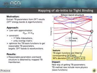
Motivation • Nano electronic devices • complicated 2D/3D geometries; • 10000 ~ 10 million atoms in the active domain; • many materials are used. • Candidate methods for device-level simulations • Ab-initio methods • Empirical methods • efficiency should be considered
simulation time and accuracy Empirical Tight Binding can be fast and accurate enough Easier for device level calculations LDA /GGA sp3s* TB Empirical TB ab-initio methods Error (compared with Experiment) GW/BSE sp3d5s* TB Depend on parameters Device-level calculations are possible Simulation time
Brief summary: empirical TB vsab-initio methods TB parameters of commonly used semiconductors are obtained. J. Jancu, et al., PRB 57 6493 T. Boykin, et al., PRB 66 125207 Issue: How to get TB parameters for new materials?
How to get TB parameters for new materials? • Traditional way: • This work: By fitting to experimental band structures. Demonstrated working for many situations Ab-initio calculations + TB parameters construction • Advantage: • less empirical; • can get TB Basis functions. • Disadvantage: • Dependent on ab-initio calculations. • Disadvantage: (for exotic materials) • insufficient experimental data; • TB basis remains unknown. • Require reliable ab-initio calculations; • GW / hybrid functional / bandgap correction; J. Jancu, etc, PRB 57 6493 T. Boykin, etc, PRB 66 125207
Method Yl,m(,) Step: ab-initio calculation Ei(k), φi,k(r), Hab-initio Ab-initio band structure Ei(k) 2. Step:Define analytical formula for TB basis functionsn,l,m (r,,) = Rn,l(r)Yl,m(,)Yl,m(,) is Tesseral function, Rn,l(r) is to be parametrized Wave functions φi,k(r)
Method (continue) Step: Parameterize Rn,l(r) gettransform matrix U: ab-initio basis TB basisn,l,m • 4. Step: • basis transformation (low rank approximation): • Hab-initio HTB • Approximate HTB by two center integrals; Iteratively optimize the TB results Step: Compare the TB results (band structure, wave functions) to ab-initio results; Measure the overlaps of basis functions; J. Slater & G.Koster PR. 94,1498(1964) A. Podolskiy & P. Vogl PRB 69, 233101 (2004)
Band structure of Silicon The Silicon is parameterized using 1st nearest neighbor sp3d5s* model. Most of the important bands agree with the DFT result! ABINIT is used to perform the DFT calculations Band gap is corrected by applying scissor operator
Basis functions and wave functions of Silicon Real space WFs of top most valence bands Radial parts of TB Basis functions High probability Si-Si bond Si Si Si Properties beyond traditional Empirical TB • TB Basis functions are obtained; • Selected TB eigen states are fitted to the corresponding DFT eigen states.
band structure of bulk MgO Application to new material MgO. (No existing reasonable parameters.) sp3d5s* model with 2nd NNs coupling is used Most of the important bands agree with the DFT result!
Strained Silicon biaxial strain ( ) Strain dependent basis functions Energy of conduction bands under Biaxial strain Energy of valence bands under Biaxial strain The behavior of strained Silicon are accurately reproduced!
conclusion • We develop a method Generating TB Parameters from ab-initio simulations • Works for typical semiconductors like Si; • Provides basis functions and TB eigen functions. • Works for new materials like MgO; • Works for more complicated materials like Strained Si.
Appendix Basis functions definition: TB Bloch functions: transform matrix U: basis transformation: