Download
1 / 30
300 likes | 420 Views
3 rd Annual 12GeV Trigger Workshop Christopher Newport University 8 July 2010 R . Chris Cuevas. Welcome! Opening comments – Dean David Doughty – CNU Workshop purpose and goals Update from 1 year ago: What have we done? Brief review of trigger requirements

E N D
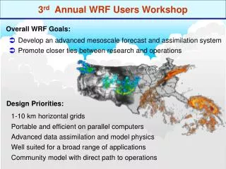
3rd Annual 12GeV Trigger Workshop Christopher Newport University 8 July 2010 R. Chris Cuevas • Welcome! • Opening comments – Dean David Doughty – CNU • Workshop purpose and goals • Update from 1 year ago: What have we done? • Brief review of trigger requirements • Identify additional requirements/features for hardware proposed at CD3 • Hardware Status • Have requirements changed for modules yet to be designed? (GTP, TS) • 3. Summary and brief overview of other sessions
Workshop Format & Goals • Four work sessions with overview presentations and plenty of time for questions and discussions! • Discussion topics are listed in the agenda for each session and I strongly encourage comments from all attendees. • The goals of this workshop are: • Discuss the most recent hardware developments • Understand and document any new features that have not been identified at CD3 and that must be implemented for the 12GeV experimental programs. • Share recent trigger ‘application’ results from existing prototype modules and also share trigger applications that are in the development stage. ** See B. Sawatzky’s & S. Boyarinov’s talk ** 2
Requirement Review • 12GeV trigger system performance requirements have been driven by the GlueX (Hall D) design. • CLAS12 (Hall B) trigger requirements are significantly different, but our trigger hardware design will support the sector geometry of CLAS12 • New requirement/proposal for a Drift Chamber Track Finding Trigger upgrade • New proposal will have an impact for global trigger hardware development but the present design implementation should support this idea. • Instrumentation electronics for 12GeV (Hall A) experiments are not included in the project scope, and Hall C requirements need to be reviewed. • SBS (Super Bigbite Spectrometer) is planning to use new trigger hardware. (Even though I do not believe it is in the cost plan) • A few 6GeV experiments will benefit from the new pipelined electronics, and provide a perfect testing environment for the pre-production modules. 3
New Requirements Listed from 2009 Trigger Workshop • Use the two trigger signals, Trig1 and Trig2 to change the mode of the flash board readout. Presently the readout mode is selected when the User programs the module before starting a ‘run’. Presently the mode does not change during a ‘run’. Using the two Trigger bits, the trigger supervisor can issue a specific readout mode for a given trigger event type. (Change mode for scaler readout data for example) • Dedicate a VXS differential pair from the TI to CTP and from the TI to the SD. Keep the I^2C link, but a differential pair will be needed to transfer data from the two switch cards at a higher rate than the I^2C allows. (The dedicated pair is not required to be a gigabit serial link.) • Add input/output signaling capabilities to the CTP and TI front panels. The number and type of signaling levels were not defined, but I/O signals will be required and allow for a number of useful features. • Global Trigger -- Implement multiple trigger partitioning “sessions”. Ed and David A. outlined a simple idea for up to 4 concurrent trigger sessions using CODA3. • 5. Global Trigger – The Trigger Supervisor will need to manage external signals for calibration systems. Presently the TS is specified to connect directly to the Global Trigger Processor and the additional input/output to pulsers or other hardware will need to be managed. 4
Brief review of 12GeV Trigger Systems Hall D-GlueX Hall B-CLAS Channel Count: ~20k ~40k Event Size: ~15kB ~6kB L1 Rate: 200kHz 10kHz L1 Data: 3GB/s60MB/s To Disk: L3, 20kHz, 300MB/s L2, 10kHz, 60MB/s 5
Hall D Construction 18 June 2010 6
Trigger Requirements Review Halls B & D • 200kHz average L1 Trigger Rate, Dead-timeless, Pipelined, 2ns bunch crossing (CW Beam) -- Hall D • Data Acquisition: at least 10kHz event rate, at least 100MB/s data rate, ‘dead-timeless’ -- Hall B • Electronics: all new equipment to achieve required performance • L1 trigger supporting streaming subsystem hit patterns and energy summing with low threshold suppression • Trigger System: reliable electron identification, multi-particle events • Scalable trigger distribution scheme (GlueX: ~30 L1 crates, ~50 total readout crates) • Low cost front-end & trigger electronics solution • Reconfigurable firmware – CLAS12 (Hall B) will use different programmable features than Hall D 7
Module Definitions From CD3 Review • Decision to use VXS (VITA 41) high speed serial backplanes • Flash ADC 250Msps ( FADC250 ) ** Version 2 nearly complete ** • This is where the trigger ‘data’ begins • Crate Trigger Processor ( CTP) ** 2 units tested in 2009 ** • Collects trigger data (SUM) from 16 FADC250 modules within one crate • Transports trigger data over fiber to Global Trigger crate • 10Gbps capability ( 8Gbps successfully tested ) • Signal Distribution ( SD) ** 2 units tested in 2009 ** • Precision low jitter fanout of ADC clock, trigger and synch signals over VXS backplane to FADC250 modules • Trigger Interface – Trigger Distribution ( TI - TD ) ** 2 units at assembly ** • Direct link to Trigger Supervisor crate • Distributes precision clock, triggers, and sync to crate SD • Manages crate triggers and ReadOut Controller events 8
Module Definitions From CD3 Review • SubSystemProcessor ( SSP ) ** 1 unit assembled ** • Collects trigger data from up to 8 front end crates. (2048 channels!) • Trigger data received on front panel with fiber transceivers • 10Gbps input capability ( 4 lanes @3.125Gbps*(8/10b) ) • 10Gpbs output stream to GTP • Global Trigger Processor ( GTP ) (FY11-12) ** Schematic phase ** • Collects trigger data from 8 SSP modules within global trigger crate • Requirement for more than 8 SSP?? • 8 SSP allows 64 crates to participate in trigger • CLAS12 may need support for at least 13 SSP • Need to design prototype to support 8 SSP • Trigger Supervisor ( TS ) (FY11-12) ** Specification complete** • New board format – VXS Payload module • Distributes precision clock, triggers, and sync to crate TI-TD • Manages crate triggers and ReadOut Controller events 9
F. Barbosa H. Dong J. Wilson E. Jastrzembski Front-End Electronics: FADC250-V1 • 16 Channel 10bit, 250Msps Flash ADC • 9 full prototype units have been tested and in use for at least 2 years. • Significant development effort and success for: • Custom firmware loaded through VME • Leading edge time extraction (62.5ps LSB) • Pulse window sum (Charge) • Zero suppression – Data minimization • “Playback” mode for system testing • Module supports 2eSST VME transfers at 200MB/s transfer rate • Large event block sizes (>100) to minimize CPU interrupt handling • VXS P0/J0 outputs 5Gbps L1 data stream (hit patterns & board sum) 4 FPGA 3 Xilinx 1 Altera • Used in existing 6GeV program: • Hall A BigBite • Upgraded Hall A Moller Polarimeter JLab-FADC250: 10
F. Barbosa H. Dong J. Wilson E. Jastrzembski Front-End Electronics: FADC250-V2 • 16 Channel 12bit, 250Msps Flash ADC • Version 2 has significant part reduction. • Consolidation of logic from 4 FPGA to 2 FPGA • VHDL firmware for VME section • Maintain original specifications • Maintain all existing features • Increase capability of trigger data transfer through additional VXS lanes and higher performance FPGA • Module supports 2eSST VME transfers at 200MB/s transfer rate • Large event block sizes (>100) to minimize CPU interrupt handling • Two units to be fabricated before end of FY10 and tested • “Orders” for pre-production units (<40) have started! 11
Front-End Electronics: FADC250 L1 Data Stream L1 Energy & Hit Processing VME Readout Energy & Time Algorithms Event #2 Event #1 Detector Input ADC 8μs ADC Sample Pipeline Trigger Input Readout Features: Raw Data mode Pulse window sum (Charge) Leading edge timing extraction (62.5ps LSB) VME-2eSST Event blocking Trigger Features: 16 ‘Hit Bits’ updated at 4ns for all channels over threshold Energy summing for 16 channels Coincidence logic for 16 channels Gigabit serial transfer through VXS to CTP Trigger #2 Trigger #1 12
Crate Trigger Processor • 2 units successfully tested in 2009!! • 2 more units will be assembled with new Virtex V FX70T that supports higher serial speeds. • Each FADC250 streams energy sum/hit to Crate Trigger Processor (CTP) • Crate Trigger Processor computes a crate-level energy sum (or hit pattern) • Computed crate-level value sent via 10Gbps fiber optics to Global Trigger Crate (32bits every 4ns) CTP Prototype: Board Energy/Hits Up to 10Gbps to CTP Fiber Optics Transceiver VXS Connectors Collect serial data from 16 FADC-250 Crate Sum/Hits 10Gbps Fiber to SSP in global trigger crate 13
Crate Level – Signal Distribution • VXS Based, 20 Slot Redundant Star Backplane • VME64x backplane w/VXS (VITA 41 Standard) provides standard with high speed serial extension (new J0 connector) • 18 Payload slots w/VME64x, 2 Switch slots • Each payload slot has 8 high speed differential pairs (10Gbps each) to both switch slots VXS Backplane Physical Layout: • Crate Level Use: • VME64x used for event readout • VXS: Low jitter clock & trigger distribution • VXS: Gigabit serial transmission for L1 data streams to switch slot for processing VXS (VITA 41 standard) VME64x + high speed serial fabric on J0 14
Crate Level – Signal Distribution (SD) -Prototype 3.47ps RMS 250MHz Clock Jitter after 150m fiber distribution • VME64x backplane w/VXS (VITA 41 Standard) provides high speed serial connections from payload slots to switch slots (Dual Star) • Supports 18 Payload slots with precision clock, synchronization, and trigger signal distribution. • Receives signals from TI and distributes common signals to each payload module ( i.e. FADC250, FADC125, F1TDC ) VXS (VITA 41 standard) VME64x + high speed serial fabric on J0 VITA 41 Switch Slot Connectors Gupta M. Taylor C. Cuevas 15
Crate Level – Signal Distribution (SD) Final Version FY10 N. Nganga M. Taylor C. Cuevas • 2 Prototype SD modules successfully tested with two crate configuration in 2009 • Specification updated to support final pair mapping for front end boards and addition of PLL jitter attenuation for clock signals. • Power circuitry has been optimized from prototype version • Specifications for synchronization, trigger signal distribution plus collection of BUSY, and management of token passing are virtually unchanged from original version. • Welcome to Mr. Nick Nganga! • Work plan for final board revision at end of FY10 and testing in FY11 16
VXS Pair Mapping 17
Level 1 & Trigger Distribution Trigger Decisions Global Trigger Crate Trigger Distribution Crate SSP SSP SSP TD TD TD SSP TD SSP SSP SSP GTP GTP SSP SSP SSP SSP SSP TI TD TD TD TD TD TD TD TD TS SD L1 Subsystem Data Streams (hits & energy) CPU CPU Fiber Optic Links TD can manage 8 TI (Crates) Fiber Optic Links SSP can manage 8 CTP (Crates) Clock Trig1 Trig2 Sync Busy 256 FADC channels/Crate VXS-Crate VXS-Crate Front-End Crates VME Readout to Gigabit Ethernet Up to 128 front-end crates 18
TID **See William Gu’s discussion at next session** • Trigger/Clock/Sync distribution/Busy • Two sided, 12-layer VME board (6Ux160mm) • PCB layout finished • PCB fabrication after independent review/check • FPGA firmware development underway • Board testing in the summer. (Virginia summer is earlier) • Module has been designed to function as Trigger Interface or Trigger Distribution • Module can be configured to function as a Trigger Supervisor (Trigger signals received on front panel I/O connector) • VXS payload board format • Provides communication from VME to SD & CTP modules via I^2C serial links. 19 11
SSP PCB Module Overview Ben Raydo 8x 10Gbps Fiber Transceivers 4x LVDS/PECL/ECL Inputs 4x LVDS Outputs 2x Bi-Directional NIM Ports Status LEDs VME Address DIP Switches DDR2 SO-DIMM (up to 4GBbyte) Jtag Power Supply Margin Header VME64x P2 VME64x P2 VXS P0 20
SSP Block Diagram Ben Raydo To GTPs (Global-Trigger-Processors) Front-Panel I/O TX: 4x LVDS RX: 4x AnyLevel (LVDS,ECL,PECL) Bidirectional: 2x NIM VXS-P0 Receives: CLK250,TRIG1,TRIG2,SYNC,LINKUP Transmits: TXDATA[3..0],Busy 2x10Gbps L1 Streams HFBR-7934 4-Channel Full Duplex 2.5Gbps Fiber Streams Clock Distribution -Distributes to all FPGAs: 50MHz, 250MHz Clocks -Local 250MHz & 50MHz -SMA 250MHz, VXS-P0 SWA or SWB 10Gbps L1 Stream • Virtex 5 - FX70T • - 4x 10Gbps Fiber Transceiver • Reed Solomon FEC Decoder • 500MB/s FX70T<->LX50T Bus • Used for VME Bridge • 4x 5Gbps FX70T->LX50T Bus • Used for L1 Streams HFBR-7934 4-Channel Full Duplex 2.5Gbps Fiber Streams 4Gbps VME Bridge HFBR-7934 4-Channel Full Duplex 2.5Gbps Fiber Streams • Virtex 5 – LX50T • - 2x 10Gbps VXS Switch Links • VME64x Interface • 500MB/s FX70T<->LX50T Bus • Used for VME Bridge • 8x 5Gbps FX70T->LX50T Bus • Used for L1 Streams • DDR2 SO-DIMM • Used for L2 dictionary From CTPs (Crate-Trigger-Processors) HFBR-7934 4-Channel Full Duplex 2.5Gbps Fiber Streams VME64x -Support for A24/A32, D32/D64 Transactions -Single Cycle, BLT, 2eSST Support 4x 5Gbps L1 Streams 4x 5Gbps L1 Streams HFBR-7934 4-Channel Full Duplex 2.5Gbps Fiber Streams 10Gbps L1 Stream • Virtex 5 - FX70T • - 4x 10Gbps Fiber Transceiver • Reed Solomon FEC Decoder • 500MB/s FX70T<->LX50T Bus • Used for VME Bridge • 4x 5Gbps FX70T->LX50T Bus • Used for L1 Streams HFBR-7934 4-Channel Full Duplex 2.5Gbps Fiber Streams 4Gbps VME Bridge HFBR-7934 4-Channel Full Duplex 2.5Gbps Fiber Streams • DD2 SO-DIMM • Up to 4GB Memory Module • <60ns Random Access Time • 3.2Gbyte/sec burst rate HFBR-7934 4-Channel Full Duplex 2.5Gbps Fiber Streams 21 8
Ben Raydo Global Trigger Processor: (GTP) • Global Trigger Processor (GTP) receives all subsystem Level 1 data streams • Trigger decisions made in GTP and distributed to all crates via the Trigger Distribution (TD) modules in the Trigger Supervisor Crate SSP Up to 8x L1 Crates per SSP SSP FCAL (Energy) SSP SSP GTP BCAL (Energy) SSP GTP TOF (Hits) SSP Start Counter (Hits) SSP Trigger Decisions to Trigger Distribution Crate Tagger (Hits) Each Connection: 8Gbps SSP->GTP (32bits every 4ns) from CTPs up to 8 SSP Modules (64 L1 Front-End Crates) 22
Virtex 5 devices available now that have high GigaBit transceiver counts capable of managing the data from up to 8 Sub-System Processors • GTP logic will effectively have all trigger data from up to 64 Level 1 crates in one FPGA. 23
Discussion Point • Questions about existing hardware designs? • What other features would be useful or have been omitted on existing prototypes? • Recognize that firmware features take significant development and test time • Must meet 12GeV construction schedules too! • Advanced question: Have requirements changed for GTP and TS modules? • What capabilities/features must these boards support? • i.e. GTP must support >12 SSP for CLAS12 • What other global trigger equations will be required? • Are there incompatibility issues with legacy readout systems? (i.e. Hall A, Hall C) • Other issues? 24
Summary • Several module designs are at the final ‘production’ revision stage: • FADC-250 • SD • CTP • Significant test effort will be needed for full multi-crate setup • Proposal exists to use new electronics for 6GeV beam test in Hall B (~Sept-11) • Real hardware prototypes, SSP, TI-D have been designed and assembled. (FY10) • Significant test work for FY11 • Plenty of engineering details (“Electronics & DAQ groups” ) remain • CODA Library development progressing for these new modules • Global Trigger Processor (GTP) and Trigger Supervisor (TS) need to be designed, • assembled and tested in FY11! • Low quantities needed but complexity will demand significant test period • DAQ Crate procurement ready for final RFP from selected manufacturers 25
Overview of other Sessions Thanks in advance to the presenters for their contributions DAQ System Update (David Abbott) Linux Front-Ends (Bryan Moffit) Trigger Interface and Distribution (William Gu) Global trigger and Commissioning (Alex Somov and Hai Dong ) Tools for high level trigger algorithms in Sub-System Processor & GTP (Ben Raydo) Recent experience with FADC-250 trigger features on PREx (Brad Swatzky) Trigger system applications for CLAS 12 (Sergey Boyarinov) 26
2 Crate Energy Sum Testing Global Sum Capture (at “SSP”): Input Signal(to 16 FADC250 Channels): Raw Mode Triggered Data (single channel shown only): • Threshold applied to global sum (80 digitized channels) produces 3 triggers. • Raw channel samples extracted from pipeline shown for 1 channel. • Runs at 250kHz in charge mode • Latency: 2.3µs(measured) + 660ns(GTP estimate) < 3µs
2 Fully Prototyped Front-End Crates SSP* TD Trigger Decision Trigger/Clock/Sync/Busy L1 Crate Sum 10Gbps Stream CPU - 6100 FADC250 FADC250 CTP#1 SD FADC250 FADC250 TI “davw1” VXS crate CPU - 6100 FADC250 CTP#2 SD FADC250 TI “davw5” VXS crate *SSP function embedded inside 2nd CTP
Example L1 Trigger cont… BCAL & FCAL <30MeV Channel Suppression (done at FADC250): <30MeV – Rejected by FADC250 FADC Channel Input: >30MeV – Accepted by FADC250 FADC L1 Sum Output: GTP Trigger Equation: Resulting L1 Acceptance Spectrum: L1 Rate < 200kHz In Signal Region: L1 Trigger Efficiency > 92%