Download
1 / 51
510 likes | 729 Views
Stages. Load instruction - lw$1, offset($2). Beq $1, $2, offset. Finalising control. Actual Op code. Final truth table. PLA implementation. Limitations of single cycle. Clock cycle identical for every instruction CPI = 1 Bound by longest instruction (load word)

E N D
Finalising control • Actual Op code
Limitations of single cycle • Clock cycle identical for every instruction • CPI = 1 • Bound by longest instruction (load word) • Inst., register, ALU, data memory, register • Not all instructions will take this long • Memory access: 8 ns • Register access: 2 ns • ALU: 4 ns
Variable timing • If we looked at a typical instruction profile, we could estimate how inefficient this scheme is: • CPU clock cycle = 600 x 25% + 550 x 10% + 400 x 45% + 350 x 15% + 200 x 5% • CPU clock cycle = 447.5 ps
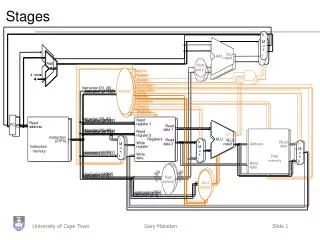
Multicycle implementation • Previously, instruction broken in to a series of steps corresponding to the functional unit operations need • Can use these steps to create a multi-cycle implementation where each step is the execution takes one clock cycle • Unit can be used more than once (on different cycles) • Can help reduce the total amount of hardware required • Trade-off with complex control
Differences • Single instruction / data memory • Single ALU • Some extra registers for buffers (more later)
Implications • Need to add more Muxs and registers (cheap) • New control signals • Write signal for each state element (PC, memory, register file, instruction register) • Read signal for memory • ALU control unit (as before) • But we can ditch two adders and memory unit
Breaking into Clock Cycles • Examine what happens in each clock cycle of each instruction to make sure we have enough elements (e.g. registers, control lines) • Registers introduced when • Value computed in one cycle and used in another • Inputs to a block change before output can be written to a state element • Mem -> ALU -> Mem
Goal of execution cycles • Balance the amount of work done each cycle to minimize the cycle time • In our case, we use 5 steps • Each step limited to • At most one ALU op • One register access • One memory access • Clock cycle will be same as the longest of these
Instruction steps • Instruction fetch • Instruction decode and register fetch • Execution, mem address completion or branch completion • Memory access or R-type write back • Write back • Using this information we can determine what control must do in each clock cycle
Instruction fetch • Load instruction from memory • IR = Memory [PC] • Set Read address mux (IorD) = 0 select instruction • Set MemRead = 1 • Increment PC • PC = PC + 4 • Set ALUSrcA = 0 get operand from IR • Set ALUSrcB = 01 get operand '4' • Set ALUOp = 00 add • Allow storing new PC in PC register
Instruction decode and fetch • Switch registers to the output of the register block • A = register [IR [25-21]] rs • B = register [IR [20-16]] rt • No signal setting required • Calculate the branch target address target PC = (sign-ext. (IR [15-0]) << 2) • Stored in the ALUOut register • Set ALUSrcB = 11 • Set ALUOp = 00 add
Memory access Execution • Step depends on the instruction • Selection performed by interpretation of the op + function field of the instruction • Calculate memory reference address • ALUOut = A + sign-ext. (IR[15-0]) • Set ALUSrcA = 1 get operand from A • Set ALUSrcB = 10 get operand from sign extension unit • Set ALUOp = 00 add
Execution II • Arithmetic-logical instruction (R-type) • ALUOut = A op B • Set ALUSrcA = 1 get operand from A • Set ALUSrcB = 00 get operand from B • Set ALUOp = 10 code from IR • Branch: if (A == B) PC = ALUOut • Set ALUSrcA = 1 get operand from A • Set ALUSrcB = 00 get operand from B • Set ALUOp = 01 subtraction • Write ALUOut to PC register
Mem access complete • Memory access • ALU controls must remain stable • Set IorD = 1 address from ALU • memory-data = memory [ALUOut] • load from memory • Set MemRead = 1 • memory [ALUOut] = B • store to memory • Set MemWrite = 1
R-type complete • Arithmetic-logical instruction complete • Register [IR [15-11]] = ALUOut • Set RegDst = 1 Select write register • Set RegWrite = 1 Allow write operation • Set MemToReg = 0 Select ALU data • ALUOp, ALUSrcA, ALUSrcB = constant
Write-back • Write data from memory to the register • Reg [IR[20-16]] = memory-data • Set RegDst = 0 Select write rt as target register • Set RegWrite = 1 Allow write operation • Set MemToReg = 1 Select Memory data • ALUOp, ALUSrcA, ALUSrcB = constant
Defining Control • Single cycle path • Construct a truth table and mapped them to logic gates • Multi-cycle • Tricky because of temporal aspect • Control must specify • Signal settings • Next step in execution • Two techniques • Finite State machines (usually graphically represented) • Microprogramming (code representation)
Finite State Machines • Consists of • Set of states • Rules for moving between states • Details • Each state has a set of asserted outputs • Those not explicitly asserted are de-asserted • States correspond to the 5 stages of execution • Each step takes one clock cycle • Initial two states are common
FSM Implementation • A register to hold current state • A block of combinational logic to determine: • Datapath signals to be asserted • The next state
Microprogramming • Design the control as a program that implements the machine instructions in terms of simpler microinstructions • For our subset, FSM are fine • For full instruction set (>100) which vary from 1 to 20 cycles more complexity is required (diagrams insufficient) • Use ideas from programming to create a simpler way to define control • Control instructions are referred to as microinstructions (as opposed to MIPS inst.)
More Microprogramming • Each instruction defines ‘the set of datapath control signals that must be asserted in a given state’ • ‘executing’ a microinstruction has the effect of asserting the specified control lines • Format • Symbolic representation of the control that is translated in to control logic • Can choose number of mInstruction fields and what control signals are affected by each field
Choices • Format is chosen to simplify representation • Improving programmer comprehension • A lot better than pure binary to specify how a Mux is set • Besides the format of the instruction, we need to figure out the order of execution
Choosing next MicroInstruction • Increment address of current mInstruction to get next mInstruction (Seq) - default • Branch to the mInstruction that begins execution of the next MIPS instruction (Fetch) • Choose next instruction based on control unit (Dispatch) • Implemented via a lookup (dispatch) table containing addresses of target mInstructions • Often multiple tables • Kind of like a switch statement
Finally - exceptions • Hardest part of control: implementing exceptions and interrupts (events other than branches that change flow of execution) • Interrupt • Unexpected change in flow of control generated by event outside processor (usually I/O device) • Exception • Any unexpected change of flow control regardless of source • Often, interrupt and exception are not distinguished
Exception Handling • Samples include • Invocation of operating system from user • Arithmetic overflow • Undefined instruction • Hardware malfunction • In our subset • Undefined instruction • Arithmetic overflow
Responding to an exception • Save address of offending instruction in EPC (exception program counter) • Transfer control to operating system with error handling code • Return to original code (using EPC) and continue. Could be: • Providing service to the user program • Coping with overflow • Stopping execution to report and error
Extra info • Operating system must know why the exception happened, not just where. Therefore could have either: • Cause register: a status register which holds field indicating reason for exception • Vectored interrupts: pair of cause and address to which control is transferred
Implication • Can perform exception handling by adding some control lines and some registers to the processor • EPC - 32 bit obviously (with EPC write control line) • Cause - 32 bit (with CauseWrite and IntCause control lines) • IntCause is 0 for undefined and 1 for overflow • Also need to write to EPC (PC - 4)
Into Practice - Pentium Datapath • Pentium based on complex (CISC) IA-32 instruction set • Some instructions take over 100 clock cycles! • Some only take 3 or 4 clock cycles • Trick is to support the long instructions without impacting the common core of instructions • Control works by • Using MicroCode for the control of long instructions • Hard-wired control for short instructions