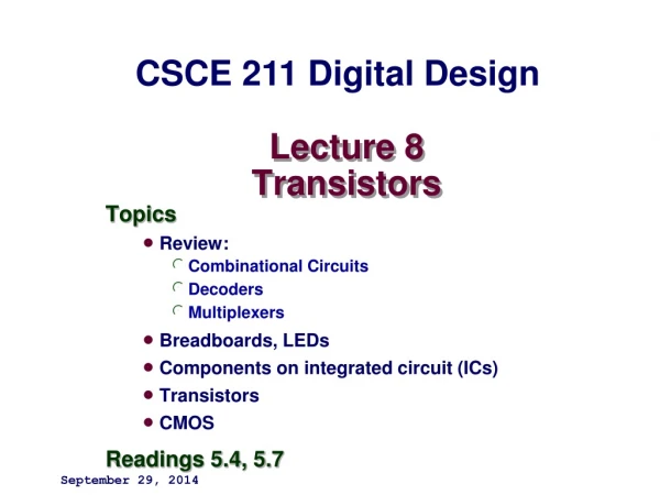
Download
1 / 48
580 likes | 1.12k Views
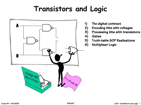
What are Transistors?. Versatile three lead semiconductor devices whose applications include electronic switching and modulation (amplification) - Transistors are miniature electronic switches. Configuration of circuit determines whether the transistor

E N D
What are Transistors? • Versatile three lead semiconductor devices whose • applications include electronic switching and modulation • (amplification) • - Transistors are miniature electronic switches. • Configuration of circuit determines whether the transistor • will serve a switch and amplifier • Building blocks of the microprocessor, which is the brain of • the computer. • - Have two operating positions- on and off. • Binary functionality of transistors enables the processing of • information in a computer. for more info. :http://goodwisher.com/
First Transistor *In the late 40s three American scientists named William Shockley, John Bardeen and Walter Brattain at Bell Labs, announced the creation of the first transistor. *The name transistor is a combination of the words transfer and resistor - a transfer resistor - a transistor. *When it was announced the name was explained; "because it is a resistor or semiconductor device which can amplify electrical signals as they are transferred through it from input to output terminals." *This, the very first transistor was called a point-contact transistor. for more info. :http://goodwisher.com/
Transistor Its is a solid state device having whose operation depends upon flow of electric charge carriers in it It is a current controlled device It consist of silicon or Ge crystal in which a layer of either p or n type is sandwiched 2 types :- PNP & NPN for more info. :http://goodwisher.com/
Bipolar Junction Transistors (BJT) Three Layers in a BJT Collector Base (very thin) has fewer doping atoms Emitter Two Types of BJT’s PNP (figure on left) operates with outgoing base current NPN (figure on right) operates with incoming base current It can be called as 2 diode connected back to back i for more info. :http://goodwisher.com/
BJT • The collector (C) collects water at the top, • the emitter (E) emits water at the bottom, • and the flow of water current is controlled by a small tap • and valve, similar to the base lead (B) of a transistor. for more info. :http://goodwisher.com/
Transistor terminals Emitter:- (left hand side section) its function is to supply majority carriers to base. It is heavily doped . Base :-(middle section) lightly doped section Collector:- (right hand side) main function is to collect majority carriers to base. It is heavily doped . The collector is the largest of the three regions; it must dissipate more heat than the emitter or base. for more info. :http://goodwisher.com/
Symbol for more info. :http://goodwisher.com/
Bipolar Junction Transistors (BJT) • The depletion layers do not have the same width, because different regions have different doping levels. The more heavily doped a region is, the greater the concentration of ions near the junction. This means the depletion layer penetrates more deeply into the base and slightly into emitter. Similarly, it penetration more into collector. The thickness of collector depletion layer is large while the base depletion layer is small for more info. :http://goodwisher.com/
Biasing Bipolar Junction Transistors (BJT) • If both the junctions are forward biased using two d.c sources, then free electrons (majority carriers) enter the emitter and collector of the transistor, joins at the base and come out of the base. Because both the diodes are forward biased, the emitter and collector currents are large. for more info. :http://goodwisher.com/
Biasing Bipolar Junction Transistors (BJT) • If both the junction are reverse biased , then small currents flows through both junctions only due to thermally produced minority carriers and surface leakage. Thermally produced carriers are temperature dependent it approximately doubles for every 10 degree celsius rise in ambient temperature. for more info. :http://goodwisher.com/
When the emitter diode is forward biased and collector diode is reverse biased then one expect large emitter current and small collector current but collector current is almost as large as emitter current. for more info. :http://goodwisher.com/
Transistor Action • When emitter diodes forward biased and the applied voltage is more than 0.7 V (barrier potential) then larger number of majority carriers (electrons in n-type) diffuse across the junction. • Once the electrons are injected by the emitter enter into the base, they become minority carriers. • These electrons do not have separate identities from those, which are thermally generated, in the base region itself. • The base is made very thin and is very lightly doped. Because of this only few electrons traveling from the emitter to base region recombine with holes. • This gives rise to recombination current. The rest of the electrons exist for more time. for more info. :http://goodwisher.com/
Transistor Action • Since the collector diode is reverse biased, (n is connected to positive supply) therefore most of the electrons are pushed into collector layer. These collector electrons can then flow into the external collector lead. for more info. :http://goodwisher.com/
Thus, there is a steady stream of electrons leaving the negative source terminal and entering the emitter region. • The VEB forward bias forces these emitter electrons to enter the base region. • The thin and lightly doped base gives almost all those electrons enough lifetime to diffuse into the depletion layer. • The depletion layer field pushes a steady stream of electron into the collector region. • These electrons leave the collector and flow into the positive terminal of the voltage source. • In most transistor, more than 95% of the emitter injected electrons flow to the collector, less than 5% fall into base holes and flow out the external base lead. • But the collector current is less than emitter current. for more info. :http://goodwisher.com/
Transistors have three terminals: Collector Base Emitter Active: Always on Ic=ß Ib Saturation :Ic=Isaturation On as a switch CUT Off :Ic=0 Off as a switch for more info. :http://goodwisher.com/
Transistor Amplifier Basics It is critical to understand the notation used for voltages and currents in the following discussion of transistor amplifiers. This is therefore dealt with explicitly ‘up front’. We will be dealing with a.c. signals superimposed on d.c. bias levels. for more info. :http://goodwisher.com/
Transistor Amplifier Basics We will use a capital (upper case) letter for a d.c. quantity (e.g. I, V). We will use a lower case letter for a time varying (a.c.) quantity (e.g. i, v) for more info. :http://goodwisher.com/
Transistor Amplifier Basics These primary quantities will also need a subscript identifier (e.g. is it the base current or the collector current?). For d.c. levels this subscript will be in upper case. (e.g. IB). We will use a lower case subscript for thea.c.signal bit (e.g. ib). And an upper case subscript for thetotal time varying signal (i.e. the a.c.signal bit plus the d.c. bias) (e.g. iB).This will be less common. for more info. :http://goodwisher.com/
Transistor Amplifier Basics It is convention to refer all transistor voltages to the ‘common’ terminal. Thus in the CE configuration we would write VCE for a d.c. collector emitter voltage and VBE for a d.c. base emitter voltage. for more info. :http://goodwisher.com/
Relation between different currents in a transistor: • The total current flowing into the transistor must be equal to the total current flowing out of it. Hence, the emitter current IE is equal to the sum of the collector (IC ) and base current (IB). That is, • IE = IC + IB for more info. :http://goodwisher.com/
The currents directions are positive directions. The total collector current IC is made up of two components. • 1. The fraction of emitter (electron) current which reaches the collector (αdc IE ) • 2. The normal reverse leakage current ICO for more info. :http://goodwisher.com/
αdc is known as large signal current gain or dc alpha. It is always positive. Since collector current is almost equal to the IE therefore αdc IE varies from 0.9 to 0.98. Usually, the reverse leakage current is very small compared to the total collector current. for more info. :http://goodwisher.com/
NOTE: The forward bias on the emitter diode controls the number of free electrons infected into the base. The larger (VBE) forward voltage, the greater the number of injected electrons. The reverse bias on the collector diode has little influence on the number of electrons that enter the collector. Increasing VCB does not change the number of free electrons arriving at the collector junction layer. for more info. :http://goodwisher.com/
Common Emitter Characteristics For the present we consider DC behaviour and assume that we are working in the normal linear amplifier regime with the BE junction forward biased and the CB junction reverse biased for more info. :http://goodwisher.com/
Common Emitter Characteristics Treating the transistor as a current node: Also: for more info. :http://goodwisher.com/
Common Emitter Characteristics Hence: which after rearrangement gives for more info. :http://goodwisher.com/
Common Emitter Characteristics Define a common emitter current-transfer ratio Such that: for more info. :http://goodwisher.com/
Common Emitter Characteristics Since reverse saturation current is negligible the second term on the right hand side of this equation can usually be neglected (even though (1- α) is small) Thus for more info. :http://goodwisher.com/
Common Emitter Characteristics We note, in passing that, if β can be regarded as a constant for a given transistor then For a practical (non-ideal) transistor this is only true at a particular bias (operating) point. for more info. :http://goodwisher.com/
Common Emitter Characteristics A small change in α causes a much bigger change in ß which means that ß can vary significantly, even from transistor to transistor of the same type. We must try and allow for these variations in circuit design. for more info. :http://goodwisher.com/
Common Emitter Characteristics For example; α = 0.98, β = 49 α = 0.99, β = 99 α = 0.995, β =199 for more info. :http://goodwisher.com/
Common Emitter Characteristics For a given transistor type data sheets may specify a range of values for more info. :http://goodwisher.com/
Common Emitter Characteristics The behaviour of the transistor can be represented by current-voltage (I-V) curves (called the characteristic curves of the device). As noted previously in the common emitter (CE) configuration the input is between the base and the emitter and the output is between the collector and the emitter. for more info. :http://goodwisher.com/
Common Emitter Characteristics We can therefore draw an input characteristic (plotting base current IB against base-emitter voltage VBE) and an output characteristic (plotting collector current Ic against collector-emitter voltage VCE) for more info. :http://goodwisher.com/
Common Emitter Characteristics We will be using these characteristic curves extensively to understand: How the transistor operates as a linear amplifier for a.c. signals. The need to superimpose the a.c. signals on d.c. bias levels. The relationship between the transistor and the circuit in which it is placed. for more info. :http://goodwisher.com/
Common Emitter Characteristics Once these basics are understood we will understand: Why we can replace the transistor by a small signal (a.c.) equivalent circuit. How to derive a simple a.c. equivalent circuit from the characteristic curves. Some of the limitations of our simple equivalent circuit. for more info. :http://goodwisher.com/
IDEAL CE INPUT (Base) Characteristics for more info. :http://goodwisher.com/
IDEAL CE INPUT Characteristics The plot is essentially that of a forward biased diode. We can thus assume VBE 0.6 V when designing our d.c. bias circuits. for more info. :http://goodwisher.com/
IDEAL CE OUTPUT (Collector) Characteristics for more info. :http://goodwisher.com/
IDEAL CE OUTPUT (Collector) Characteristics Avoid this saturation region where we try to forward bias both junctions for more info. :http://goodwisher.com/
IDEAL CE OUTPUT Avoid this cut-off region where we try to reverse bias both junctions (IC approximately 0) for more info. :http://goodwisher.com/
IDEAL CE OUTPUT (Collector) Characteristics The plots are all parallel to the VCE axis (i.e. IC does not depend on VCE) The curves strictly obey IC = βIB In particular IC = 0 when IB = 0. We shall work with the ideal characteristic and later on base our a.c. equivalent circuit model upon it. for more info. :http://goodwisher.com/
ACTUAL CE OUTPUT Characteristics IB = for more info. :http://goodwisher.com/
ACTUAL CE OUPUT Characteristics Salient features are: The finite slope of the plots (IC depends on VCE) A limit on the power that can be dissipated. The curves are not equally spaced (i.e β varies with base current, IB). for more info. :http://goodwisher.com/