Download
1 / 25
290 likes | 557 Views
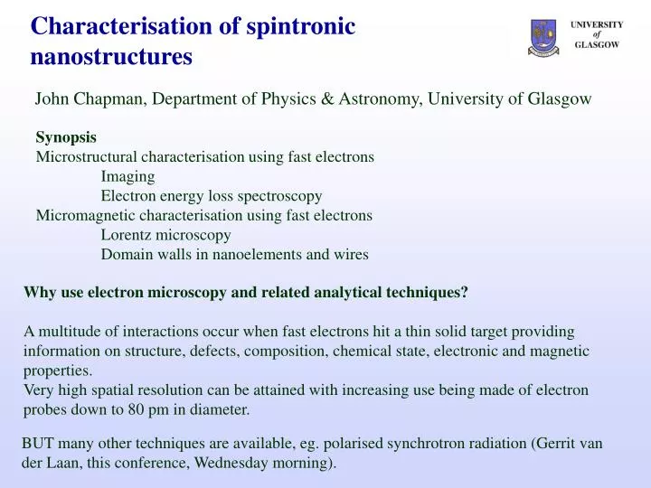
Characterisation of spintronic nanostructures. John Chapman, Department of Physics & Astronomy, University of Glasgow. Synopsis Microstructural characterisation using fast electrons Imaging Electron energy loss spectroscopy Micromagnetic characterisation using fast electrons

E N D
Characterisation of spintronic nanostructures John Chapman, Department of Physics & Astronomy, University of Glasgow Synopsis Microstructural characterisation using fast electrons Imaging Electron energy loss spectroscopy Micromagnetic characterisation using fast electrons Lorentz microscopy Domain walls in nanoelements and wires Why use electron microscopy and related analytical techniques? A multitude of interactions occur when fast electrons hit a thin solid target providing information on structure, defects, composition, chemical state, electronic and magnetic properties. Very high spatial resolution can be attained with increasing use being made of electron probes down to 80 pm in diameter. BUT many other techniques are available, eg. polarised synchrotron radiation (Gerrit van der Laan, this conference, Wednesday morning).
HR image BF image DF image TEM images through sputtered magnetic films Commonly used imaging modes: bright field (BF), dark field (DF), high resolution (HR), high angle annular dark field (HAADF)
Cross-sectional TEM images through spin tunnel junctions Specimens courtesy of P P Freitas, INESC
TiWN2 150Å Al 3000Å x TiWN2 150Å Ru Ru x Ta 30Å MnIr 250Å REFERENCE Pinned High blocking T CoFeB 30Å MnIr MnIr Ru 8Å MnIr CoFeB 40Å Al 9 +Ox CoFeB 30Å NiFe 25Å STORAGE Weakly pinned Low blocking T MnIr 80Å NiFe 25Å CoFeB 30Å Al 9 +Ox CoFeB 40Å TiWN2 REFERENCE Pinned High blocking T Ru 8Å GeSbTe CoFeB 30Å MnIr 250Å 20 nm NiFe 50Å Ta 90Å x AlOx AlOx TiWN2 150Å x Thermal Barrier GeSbTe 250Å x TiWN2 150Å Buffer Cross-sectional TEM image through a double spin tunnel junction structure Specimen courtesy of P P Freitas, INESC
Electron energy loss spectrometer X-ray detector Probe forming lens Specimen High angle annular dark field detector (HAADF) Schematic scanning transmission electron microscope (STEM)
zero loss peak x~60 gain Mn L2,3-edges Fe L2,3-edges Co L2,3-edges 1st plasmon peak x20 gain -200 0 200 400 600 800 1000 Energy Loss (eV) Introduction to electron energy loss spectroscopy
Spectrum imaging • 3-D data set • x by y pixels • Full spectrum at each pixel • EELS, EDX • Can be extended to N-dimensional data set
ADF and EELS spectrum image centred around the oxide layer of an STJ O K 532eV Fe L 708eV Ni L 855eV Mn L 640eV Co L 779eV SiO2 A B A x (nm) B E (eV) Specimen courtesy of P P Freitas, INESC
EELS spectrum image centred around the oxide layer – normal region SiO2
EELS spectrum image centred around the oxide layer - anomalous region SiO2
Some magnetic imaging modes in the (S)TEM • There are several different modes of Lorentz microscopy. • Category I reveals domain walls (DWs) • Category II is sensitive to domain contrast leading to vector induction maps • Category III yields interferograms mapping flux lines. DPC images Foucault images Fresnel image Coherent Foucault image
probe-forming aperture scan coils a B B o o specimen b L de-scan coils post- specimen lenses quadrant detector Fresnel and differential phase contrast (DPC) imaging modes
M M Variation of cross-tie density with field parallel to the element long axis – Fresnel imaging Schematic of a cross-tie wall • Cross-tie density depends on the domain width • The domain width can be controlled by the proximity of the wall to the element edge when driven towards the edge by an external field
Cross-tie walls in permalloy elements – DPC imaging • The cross-tie geometry is remarkably • stable • The size of the basic cross-tie unit can • change by at least a factor of 10 for • constant thickness elements • Domain walls in small elements do not • act as rigid objects
Vortex DW Transverse DW plan view ? If constrain geometry further by forming a wire (width, w < 1 μm) then obtain head-to-head/tail-to-tail DWs due to the strong shape anistropy: ? t w ? Domain walls in wires
125 nm 250 nm 500 nm Chirality control through pad geometry selection • FIB milled structure, 20nm NiFe • Asymmetric notch to pin DWs • Inject DWs from pad attached to nanowire • Pad shape optimised to control DW chirality Micromagnetic simulations cw rotation in pad ccw rotation in pad +18 % greater energy
Realisation of chirality control Fresnel mode images Hsat 500nm Hsat Asymmetry allows choice of vortex chirality in pad
Injection of vortex domain walls Outward direction Happ Happ 0 Oe Hinject = +96 Oe Hde-pin=+153 Oe DE-PINNING INJECTION Return direction Hde-pin=-105 Oe 0 Oe Hinject = -71 Oe Happ Happ
t w Head-to-head domain wall structures in magnetic wires Vortex DW degrees of freedom: • head-to-head/tail-to-tail • chirality • polarisation Transverse DW degrees of freedom: • head-to-head/tail-to-tail • up/down
Asymmetric transverse DW Additional asymmetry degrees of freedom Head-to-head domain wall structures in magnetic wires • DW type dictated by wire width, w, and thickness, t • Asymmetric transverse DW predicted by Nakatani et al. [1] [1] Nakatani et al., J. Magn. Magn. Mater. 290-291, 750 (2005)
Curved permalloy wires containing an anti-notch Permalloy wire wire width 500 nm; wire thickness 8 nm Radius of curvature of wire: ~50 µm Radius of protuberance: 250 nm Specimen courtesy of C. Sandweg, TU Kaiserslautern, Germany
Asymmetric transverse domain wall in a 10 nm thick permalloy wire
High resolution induction maps of the effect of an applied field on an aTDW at an anti-notch The induction maps were generated from pairs of DPC images; resolution ≈25 nm
Summary • A combination of different imaging and analytical techniques provides a wealth of information about complex multilayers of the kind under investigation for spintronic applications. • Electron probe techniques, particularly HAADF imaging and EELS are very effective for characterising interfaces and edges, and have atomic resolution capability. However, layer roughness of most metal-based spintronic multilayers preclude information at this level being obtained. • Lorentz microscopy is a versatile tool for magnetic imaging of elements and wires. In- situ studies can be carried out and quantitative magnetic induction distributions determined. • Domain wall structures can and do easily change. The fact that TEM images can be generated in real time makes it particularly powerful for studying the effects of constrictions, edge roughness and the microstructure of the wires themselves.
Acknowledgements Stephen McVitie, Maureen MacKenzie, Damien McGrouther, Nils Wiese, John Weaver, Chris Wilkinson (University of Glasgow) Paulo Freitas, Susanna Cardoso (INESC) Stefan Muller (MPI, Leipzig), Felix Otto (Bonn) Britta Leven, Christian Sandweg, Burkard Hillebrands (Technical University of Kaiserslautern) Members of the UK Spin@RT consortium Financial support EPSRC, EU MCRTN SPINSWITCH, EU MCRTN MULTIMAT