Download
1 / 98
1.21k likes | 1.65k Views
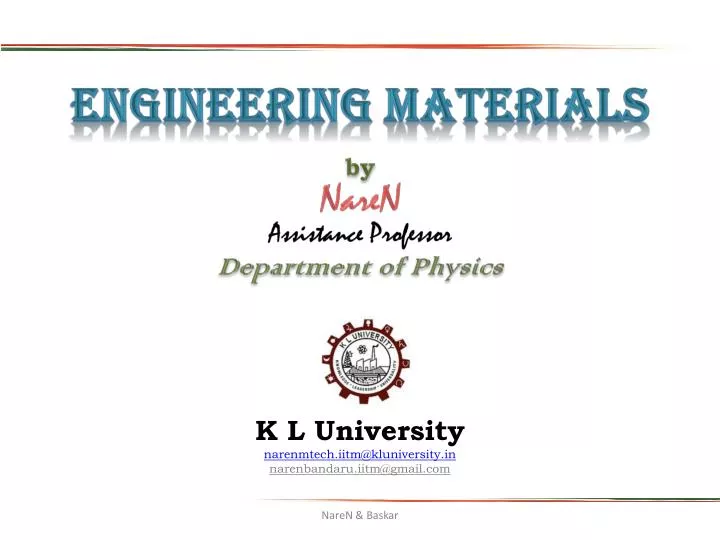
Engineering Materials. by NareN Assistance Professor Department of Physics. K L University narenmtech.iitm@kluniversity.in narenbandaru.iitm@gmail.com. Electrical Properties. Their responses to an applied field. Electrical Properties of materials . Electrical Conduction

E N D
Engineering Materials • by • NareN • Assistance Professor • Department of Physics K L University narenmtech.iitm@kluniversity.in narenbandaru.iitm@gmail.com NareN & Baskar
Electrical Properties Their responses to an applied field Electrical Properties of materials • Electrical Conduction • Electron Band Structure of a materials Materials Metals Semiconductors Insulators Dielectric characteristics NareN & Baskar
Electrical Conduction in Metals • Ohm’s Law • At constant temperature the current flowing through a conductor is directly proportional to the potential difference across the ends of the conductor. • Macroscopic form NareN & Baskar
Electrical Conduction in Metals Resistance • The opposing force offered by the material to the flow of current. • Depends on • Nature of the material (ρ). • Temperature. • Geometry/ dimensions (length L, area of cross section A) R = r (L/A) NareN & Baskar
surface area of current flow current flow path length Electrical Conduction in Metals Resistivity • It is a material property. • It defines how difficult is it for current to flow. • Geometry independent. • Temperature dependent. NareN & Baskar
Electrical Conduction in Metals Examples of Resistivity (ρ) • Ag (Silver): 1.59×10⁻⁸ Ω·m • Cu (Copper): 1.68×10⁻⁸ Ω·m • Graphite (C): (3 to 60)×10-5 Ω·m • Diamond (C): ~1014 Ω·m • Glass: ~1010 - 1014 Ω·m • Pure Germanium: ~ 0.5Ω·m • Pure Silicon: ~ 2300Ω·m NareN & Baskar
Electrical Conduction in Metals Current Density (J) • It is the current flowing through unit area of cross section. NareN & Baskar
Electrical Conduction in Metals Ohm's Law -- Microscopic Form NareN & Baskar
Electrical Conduction in Metals Experimental verification of ohm’s law NareN & Baskar
Electrical Conduction in Materials Electrical conductivity varies between different materials by over 27 orders of magnitude, the greatest variation of any physical property Metals: > 107 (.m)-1 Semiconductors: 10-6 < < 105 (.m)-1 Insulators: < 10-6 (.m)-1 NareN & Baskar
Energy Band Structures in Solids NareN & Baskar
Energy Band Structures in solids • In most of solids conduction is by electrons. • σ depend on no. of electrons available • The no. of electrons available for conduction depends on • Arrangement of electrons states or levels with respect to energy. • The manner in which these states are occupied by electrons. • Current carriers • electrons in most solids • ions can also carry (particularly in liquid solutions) NareN & Baskar
Energy Band Structures in solids IONIZATION If a sufficient amount of energy is absorbed by an electron, it is possible for that electron to be completely removed from the influence of the atom For ionization to take place, there must be a transfer of energy that results in a change in the internal energy of the atom. NEGATIVE ION • Isolated Atom An atom having more than its normal amount of electrons acquires a negative charge POSITIVE ION The atom that gives up some of its normal electrons is left with fewer negative charges than positive charges NareN & Baskar
Energy Band Structures in solids When atoms are spaced far enough apart • Gas: • Very little influence upon each other, and are very much like lone atoms. • Solid : • The forces that bind these atoms together greatly modify the behavior of the other electrons. • One consequence of this close proximity of atoms is to cause the individual energy levels of an atom to break up and formbands of energy. • Discrete (separate and complete) energy levels still exist within these energy bands, but there are many more energy levels than there were with the isolated atom. NareN & Baskar
Energy Band Structures in solids • The difference in the energy arrangement between an isolated atom and the atom in a solid. • Notice that the isolated atom (such as in gas) has energy levels, whereas the atom in a solid has energy levels grouped into ENERGY BANDS. NareN & Baskar
Energy Band Structures in solids NareN & Baskar
Energy Band Structures in solids NareN & Baskar
WHY ENERGY BANDS ARE FORMED? NareN & Baskar
Electronic Band Structures • Electrons of one atom are perturbed by the electrons and nuclei of the adjacent atoms. • Results in splitting of atomic states into a series of closely spaced electron states to from what are called ELECTRON ENERGY BAND. • Extent of splitting depends on interatomic separation. NareN & Baskar
Electronic Band Structures Schematic plot of electron energy versus interatomic separation for an aggregate of 12 atoms Upon close approach, each of the 1s and 2s atomic states splits to form an electron energy band consisting of 12 states. NareN & Baskar
Electronic Band Structures • Valence band – filled – highest occupied energy levels • Conduction band – empty – lowest unoccupied energy levels At Equilibrium spacing : Band formation may not occur NareN & Baskar
Electronic Band Structures • With in each band the energy states are discrete. • No. of states with in each band will equal the total of all states contributed by the N atoms. • s band consists of N states • p band consists of 3N states • Electrical properties of a solid depends on its electron band structure. NareN & Baskar
Electronic Band Structures NareN & Baskar
Energy Band Structure Baskar,NareN,G.S
Electronic Band Structures The concept of energy bands is particularly important in classifying materials as conductors, semiconductors, and insulators. An electron can exist in either of two energy bands, the conduction band or the valence band. All that is necessary to move an electron from the valence band to the conduction band so it can be used for electric current, is enough energy to carry the electron through the forbidden band. The width of the forbidden band or the separation between the conduction and valence bands determines whether a substance is an insulator, semiconductor, or conductor. Baskar,NareN,G.S
Electronic Band Structures Energy level diagrams to show the difference between insulators, semiconductors, and conductors. Baskar,NareN,G.S
Electronic Band Structures Baskar,NareN,G.S
Electronic Band Structures The energy corresponding to the highest filled state at 0 K is called the Fermi energy Cu-3d10 4s1- One 4s electron Mg-12-Two 3s electrons Baskar,NareN,G.S
Conduction in Solids Presence of an electric field : • Accelerated • Electrons with energies greater than the Fermi energy ( Ef) Conduction process • Free electrons • Holes – SMC & Insulators • Electrical conductivity is a direct function no: of free electrons and holes. • Distinction between conductors and nonconductors (insulators and semiconductors) ----- lies in the numbers of these free electron and hole charge carriers. Baskar,NareN,G.S
Conduction in Metals Metals • For an electron to become free, it must be excited or promoted into one of the empty and available energy states above Ef . • Very little energy is required to promote electrons into the low-lying empty states. • Electrons are not locally bound to any particular atom Baskar,NareN,G.S
Partially filled band Overlapping bands Energy Energy empty band empty GAP band partly filled filled band band filled states filled states filled filled band band Conduction in Metals • Metals (Conductors): -- Thermal energy puts many electrons into a higher energy state. • Energy States: -- for metals nearby energy states are accessible by thermal fluctuations. Baskar,NareN,G.S
Conduction in Insulators & SMC • Empty States adjacent to the top of the filled valence band are not available. • To become free, therefore, electrons must be promoted across the energy band • and into empty states at the bottom of the conduction band. • This is possible only by supplying to an electron the difference in energy between these two states, which is approximately equal to the band gap energy Eg Excitation energy Nonelectrical source Heat or light Number of electrons excited thermally (by heat energy) depends --> 1.Energy band gap width 2.Temperature Baskar,NareN,G.S
Conduction in Insulators & SMC 1. Eg is small – conduction is high 2. Eg is large – conduction is low At a given Temperature SMC – Narrow Insulators -- Widely Width of the band gap Increasing the temperature Thermal energy increases Conductivity increases No of electrons excitation more Baskar,NareN,G.S
Conduction in Insulators & SMC Bonding valence electrons are not as strongly bound to the atoms covalent Semiconductors electrons are more easily removed by thermal excitation ionic or strongly covalent valence electrons are tightly bound Insulating material electrons are highly localized Baskar,NareN,G.S
Energy Energy empty empty band band ? GAP GAP filled filled valence valence band band filled states filled states filled filled band band Conduction in Insulators & SMC Width of the band gap • Insulators: -- Higher energy states not accessible due to gap (> 2 eV). • Semiconductors: -- Higher energy states separated by smaller gap (< 2 eV). Baskar,NareN,G.S
Conduction in Insulators & SMC Width of the band gap Baskar,NareN,G.S
Electron Mobility Absence of Electric field: (E=0) 1. Electrons move randomly through out the crystal in conductors 2. Net current – ZERO ( any direction) 3. No Drift velocity Presence of Electric field: 1.Electrons are accelerated in a single direction 2.This acceleration is opposed by the internal damping forces or frictional forces. due to scattering of electrons by imperfections Baskar,NareN,G.S
Electron Mobility imperfection's 1. Impurity atoms 2. Vacancies 3.Dislocations 4.Thermal vibration 5.Interstitial atoms Baskar,NareN,G.S
Electron Mobility Each Scattering or Collision occurs: A) e- losses kinetic energy Transfer to the lattice of metal B) Changes its direction of motion e- - lattice scattering 1. Existence of resistance 2. Warming up of the metals Ex: Electrical heaters Baskar,NareN,G.S
Electron Mobility • Electronsmove randomly but with a net drift in the direction opposite to the electric field. scattering phenomenon resistance used to describe 1. mobility of an electron 2. drift velocity It is represents the average electron velocity in the direction of the force imposed by the applied field. It is directly proportional to the electric field. vd = eE e– electron mobility [m2/V-s]. Baskar,NareN,G.S
Electron Mobility • Electrical conductivity proportional to number of free electrons per unit volume, Ne, and electron mobility, e = Nee e Nmetal >> Nsemi metal >semi metal >> semi Baskar,NareN,G.S
Electrical resistivity of metals Baskar,NareN,G.S
Electrical resistivity of metals Metals are extremely good conductors of electricity large numbers of free electrons excited into empty states above the Fermi energy Discuss conduction in metals in terms of the resistivity • crystalline defects serve as scattering centers for conduction electrons increasing their number raises the resistivity concentration of these imperfections temperature, composition Baskar,NareN,G.S
Electrical resistivity of metals total = thermal+impurity+deformation experimentally Matthiessen’s rule The electrical resistivity versus temperature for copper and three copper–nickel alloys, one of which has been deformed. Influence of Temperature : • pure metal and all the copper–nickel alloys • Resistivity rises linearly with temperature * T Vibrations and lattice defects electron scattering increases Baskar,NareN,G.S
Electrical resistivity of metals Influence of Impurities Impurity resistivity ρiis related to the impurity concentration Ciin terms of the atom fraction (at%100) where A is a composition-independent constant (impurityand host metals) • Two-phase alloy consisting of α and β phases where the V’s and ρ’s represent volume fractions and individual resistivities for the respective phases. • The influence of nickel impurity additions on the room temperatureresistivity of copper Baskar,NareN,G.S
Electrical resistivity of metals Influence of Plastic Deformation Raises the electrical resistivity Result of increased numbers of electron-scattering dislocations. • Its influence is much weaker than that of increasing temperature or the presence of impurities. Baskar,NareN,G.S
Electrical characteristics of commercial alloys Silver Best material for electrical conduction Very expensive Copper To achieve low resistance Remove gases included in metal Soft material Mechanical strength CuBe is used Aluminium Weight More resistant to corrosion Baskar,NareN,G.S
Electrical characteristics of commercial alloys Furnace heating elements high electrical resistivity energy loss by electrons dissipated as heat energy Ex: Nichrome, a nickel–chromium alloy Baskar,NareN,G.S
Semiconductors Semiconductors have a resistivity/resistance between that of conductors and insulators Their electrons are not free to move but a little energy will free them for conduction Their resistance decreases with increase in temperature Electrical properties are extremely sensitive to the presence of impurities. Baskar,NareN,G.S
INTRINIC SEMICONDUCTORS Baskar,NareN,G.S