Download
1 / 69
700 likes | 952 Views
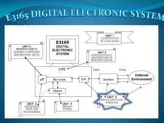
Microprocessor System Design Input / Output Peripheral Interfacing. Omid Fatemi (omid@fatemi.net). Outline. Peripheral devices Input devices Output devices 8 bit / 16-bit IO Simple Input device - interfacing switches Simple Output device - interfacing LEDs 8255 PPI 8255 modes

E N D
Microprocessor System DesignInput / OutputPeripheral Interfacing Omid Fatemi (omid@fatemi.net)
Outline • Peripheral devices • Input devices • Output devices • 8 bit / 16-bit IO • Simple Input device - interfacing switches • Simple Output device - interfacing LEDs • 8255 PPI • 8255 modes • 16-bit data bus to 8-bit peripherals or memory devices
Peripheral • is an input and/or output device • like a memory chip, it is mapped to a certain location (called the port address) • unlike a memory chip, a peripheral is usually mapped to a single location
Output Device • like a memory chip, you can write to an output device • You can write to a memory chip using the command mov [bx], al • You can write to an output device using the command out dx, al
Input Device • like a memory chip, you can read from an input device • You can read from a memory chip using the command mov al, [bx] • You can read from an input device using the command in al, dx
Memory mapped vs. peripheral • Same instruction vs. independent instruction • Entire address bus vs. part of address bus • Same control signals vs. independent • More IO ports vs. 65536 ports • More commands and operations • Uses memory space
Format 1 IN AL, port# Or OUT port#, AL Example: BACK: IN AL,22H CMP AL, 100 JNZ BACK Format 2 MOV DX,port#IN AL, DX Or MOV DX, port#OUT DX, AL Two formats for IN / OUT
8088 case: MOV DX, 648HOUT DX, AX ;AX = 76A9H Address bus and ALE Low byte (A9), IOW Setup time Address (649) and ALE High byte (76), IOW Setup time 8086 case: MOV DX, 648HOUT DX, AX ;AX = 76A9H Address bus and ALE Word (76A9), IOW Setup time 8bit vs 16bit IO
Creating a Simple Output Device • Use 8-LED’s
Use 8 LED’s A19 A18 : A0 : mov al, 55 out dx, al : : : D7 D6 D5 D4 D3 D2 8088 D1 Minimum D0 Mode IOR IOW
Creating a Simple Output Device • Use 8-LED’s • Use a chip and an address decoder such that the LED’s will respond only to the command out and a specific address (let’s assume that the address is F000)
A0 B0 A1 B1 A2 B2 A3 B3 A4 B4 74LS245 A5 B5 A6 B6 A7 B7 E DIR 5V A A A A A A A A A A A A A A A A IOW 1 1 1 1 1 1 9 8 7 6 5 4 3 2 1 0 5 4 3 2 1 0 Use of 74LS245 and Address Decoder A19 A18 : A0 D7 D6 D5 D4 D3 D2 8088 D1 Minimum D0 Mode IOR : mov al, 55 mov dx, F000 out dx, al : IOW
Creating a Simple Output Device • Use 8-LED’s • Loses the data • Solution? • Use a chip and an address decoder such that the LED’s will not only respond to the command out and a specific address (let’s assume that the address is F000) but will also latch the data
D0 Q0 D1 Q1 D2 Q2 D3 Q3 D4 Q4 74LS373 D5 Q5 D6 Q6 D7 Q7 LE OE Use of 74LS373 and Address Decoder A19 A18 : A0 D7 D6 D5 D4 D3 D2 8088 D1 Minimum D0 Mode IOR : mov al, 55 mov dx, F000 out dx, al : IOW A A A A A A A A A A A A A A A A IOW 1 1 1 1 1 1 9 8 7 6 5 4 3 2 1 0 5 4 3 2 1 0
Creating a Simple Input Device • Use 8-Switches (keys) • Use a chip and an address decoder such that the keys will be read only to the command in and a specific address (let’s assume that the address is F000) • How to interface a switch to computer?
A0 B0 A1 B1 A2 B2 A3 B3 A4 B4 74LS245 A5 B5 A6 B6 A7 B7 E DIR Use of 74LS245 and Address Decoder 5V A19 A18 : A0 D7 D6 D5 D4 D3 D2 8088 D1 Minimum D0 Mode IOR : mov dx, F000 in al, dx : IOW A A A A A A A A A A A A A A A A IOR 1 1 1 1 1 1 9 8 7 6 5 4 3 2 1 0 5 4 3 2 1 0 Same address for input and output?
How do you know if a user has pressed a button? • By Polling • By Interrupt
Polling mov dx, F000 in al, dx L1: cmp al, FF je L1 : :
Output Port Design T1 – T4 of OUT 99H, AL ?
Input Port Design T1 – T4 of IN AL, 5FH ?
Modes of Operation • Mode 0 – simple input or output • Mode 1 – input or output with handshaking • Mode 2 – bideirectional IO with handshaking
Example for BSR • Program 8255 for the following • A) set PC2 to high • B) Use PC6 to generate a square wave of 66% duty cycle • Solution • A) • MOV AL, 00000101BOUT 93H,AL • B) • MOV AL, 0xxx1101OUT 93H, ALCALL DelayCALL DelayMOV AL, 0xxx1100OUT 93H, ALCALL DelayJMP AGAIN
Output with handshake • #OBFa : • CPU has written a byte • #ACKa: • Data has been picked up by receiving device • INTRa: • After rising edge of #ACKa • INTEa (interrupt enable) • Internal flipflop • Controlled by PC6
Interrupt vs. Polling • CPU is interrupted whenever necessary • CPU can serve many devices • Require more hardware
Input with handshake • #STB (in): • Device provides data to an input port • IBF (out): • Data has been latched by 8255 • INTR (out): • After activation of IBF • INTE (interrupt enable) • Internal flip-flop • Controlled by PC4 and PC2
Use of 8255 ports in PC MOV AL,99H OUT 63, AL
80x86 family • 16-bit Processors • 8088 (8-bit data / 20-bit address) • 8086/186 (16-bit data / 20-bit address) • 80286 (16-bit data / 24-bit address) • 32-bit Processors • 80386 (16/24 or 32/32 common) • 80486 (32/32), Pentium, PII (64/32) • Pentium Pro, II, III, IV (64/36) • PPC 60x (32 or 64/32) • All 80x86 processors use a 16-bit address for i/o
8 And 16 bit Organizations • 8088 • Data is organized into byte widths • The 1MB memory is organized as 1M x 8-bits • 8086/80186 • Data is organized into word widths • The 1MB memory is organized as 512kB x 16-bits • 80286/80386SX • Data is organized into word widths • The 16MB memory is organized as 8MB x 16-bits
32 and 64 bit Organizations • • 80386DX/80486 • – Data is organized into double word widths • – The 4GB memory is organized as 1GB x 32-bits • • Pentium Pro/Pentium 1-4 • – Data is organized into quad word widths • – The 4GB memory is organized as 512MB x64-bits • (on P2-4, actual address bus is 36 bits)
Little Endian / Big Endian for the 68000: MOVE.W #513, D0 ; move value 513 into the lower 16 bits of D0 MOVE.W D0,4 ; store the lower word of D0 into memory 4 for the 80x86: MOV AX,513 ; load AX (16 bits), with the value 513 MOV [4],AX ; store AX into memory 4
Memory Alignment in 16-bit Micro • We have 16-bit data bus • Why not use it for memory access. • 1M byte of memory is organized as: • 512K * 16 bit • The memory is word-aligned • Access to even addresses is aligned and simple • Example: 0102H and 0304H stored in [4H] What happens on mov AX,[4]? What happens on mov AX,[5]? Motorola family of the MC680x0 forbidsnon-aligned access
Memory Bank Select • 8086/186/286/386SX has 16 Data Lines D15-D0 • 6264 Only has 8 I/O7 – I/O0 • Must Use a “Memory Bank” • 1 SRAM for Storing Bytes with “Even Addresses” (… 0 2 ) • 1 SRAM for Storing Bytes with “Odd” Addresses” (… 1 3 ) • 8086 has BHE Control Signal – (Bank High Enable) • Can Use Combination of A0 and BHE to Determine Type of Access • BHE A0 Access Type • 0 0 1 word (16-bits) • 0 1 Odd Byte (D15-D8) • 1 0 Even Byte (D7-D0) • 1 1 No Access
AX 3F1C A19 7FFFF 36 BX 0023 A18 A18 7FFFE 25 CX 0000 : : 7FFFD 19 DX FCA1 A0 A0 : : 20023 13 D7 D7 CS XXXX 20022 7D : : SS XXXX 20021 12 D0 D0 DS 2000 20020 29 ES XXXX MEMR RD : : MEMW WR 00001 95 BP XXXX CS 00000 23 SP XXXX SI XXXX 7FFFF 12 DI XXXX A18 7FFFE 98 : 7FFFD 2C IP XXXX A0 : : 20023 33 D7 20022 45 20021 92 D0 20020 A3 : : 00001 D4 00000 97 Interfacing two 512KB Memory to the 8088 Microprocessor (review) : RD WR CS