Download
1 / 29
290 likes | 293 Views
This paper presents a 150GHz CMOS amplifier with high gain and output power. The amplifier utilizes dummy-prefilled microstrip lines to optimize performance. Measurement results and potential applications beyond 100GHz are discussed.

E N D
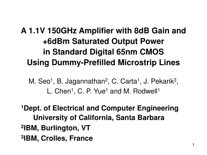
A 1.1V 150GHz Amplifier with 8dB Gain and +6dBmSaturated Output Power in Standard Digital 65nmCMOS Using Dummy-Prefilled Microstrip Lines M. Seo1, B. Jagannathan2, C. Carta1, J. Pekarik3, L. Chen1, C. P. Yue1 and M. Rodwell1 1Dept. of Electrical and Computer Engineering University of California, Santa Barbara 2IBM, Burlington, VT 3IBM, Crolles, France
Outline • Introduction • “Dummy-Prefilled” Microstrip Line • Structure and Modeling • Design and Simulation • Measurement Results
Beyond 100GHz: What Applications? O2 94GHz 140GHz 220GHz • Communication • Outdoor, indoor • Imaging (Passive, active) • Security • All-weather radar • Medical Attenuation (dB/km) H2O H2O O2 Frequency (GHz)
Beyond 100GHz: Why CMOS? • Low-cost • Low-power • Large-scale Integration → Parallelism • Large monolithic phased array, imager. • RF/mm-wave, IF/analog, DSP on a same die. • System-on-chip • Digital calibration of RF/analog circuit imperfections, process variations. • Reconfigurability and adaptability
What Challenges in 150GHz CMOS Amp? • Low available FET gain, Low Supply Voltage • Careful FET layout & sizing • Multi-stage Common-Source • Modeling uncertainties • Simple matching topology with microstrip (MS) lines • Automatic “dummies” alter MS-line characteristics • Propose “Dummy-prefilled” MS-line • Characterization • Full 2-port on-wafer TRL calibration
FET Layout • Finger design: Reduce Rg,ext and Cgd (WF=1um) • Wiring multiple fingers: Parallel versus Series Parallel gate feed (PGF) Maximum Stable Gain (dB) Series gate feed (SGF) 10x1um/65n 100 200 300 Frequency (GHz)
“Microstrip Line” in Nanoscale CMOS • “Automatic” dummies/holes to meet metal density rules. • Line capacitance increases • ΔC depends on E-field orientation → Anisotropic • Direct E/M simulation nearly impossible Signal Line Ground plane
Signal Line Signal Line Signal Line Possible Shapes of Dummy Pre-fillers • “LINE” dummies • Parallel to current flow dummies • “LINE” dummies • Perpendicular to current flow • “SQUARE” dummies • No preferred direction of current flow
Reducing Complexity in E/M Sim E/M simulation feasible by significantly reducing # of dummies W S Dummy Pre-fillers Signal Signal Dummy-free uniform dielectric with adjusted diel. constant E-field lines ε ε’ Successive dummy-layer substitution by parallel-plate capacitor simulation
56% Fill W:S = 3:1 25% Fill W:S = 1:1 Line Inductance/Capacitance vs Fill Ratio L per unit length (317nH/m w/o fillers) +32% +17% C per unit length (103pF/m w/o fillers)
M1 M2 via Ground Plane Construction • Solid GND plane not allowed • Put holes, and strap M1 & M2 + Where current flow is uniform (e.g. under MS-line) Where current flow is not uniform (e.g. under bends, T-junction, radial stubs)
THRU-REFL-LINE (TRL) Calibration Half THRU • REFL & LINE need not be accurately known • Measurements normalized to the line impedance (1) THRU Reference plane 450um (2) REFL (Open, short, etc) ΔL (3) LINE (ΔL= 90 deg @center freq) Amplifier Test
3-Stage 150GHz Amplifier: Schematic V2 V3 All TL’s: Z0= 51.2 W=10u (25% fill) • No DC block: Forces VGS=VDS for M1 & M2, but eliminates loss and modeling uncertainties associated with DC-block cap • FET size is chosen for low matching loss • Radial stub for lower loss than quarter-wave TL Radial stub TL1 TL2 TL3 TL4 V4 M1 M2 M3 V1 30u/65n 30u/65n 30u/65n Amplifier Half THRU Half THRU
FET Sizing constant-g circle (20mS) S22* (g22 g11) Z0 S11 constant-Q circle Large FET Small FET Conjugate input/output/inter-stage match with shunt tuning stubs only.
0.65V 1.1V Simulated 150-GHz Amplifier Gain PDC= 25mW Radial stub (45deg opening) AC short S21 (dB) Open-stub Z0=34, W=20u ¼λ Open-stub Z0=51, W=10u ¼λ Frequency (GHz)
Die Photograph Dummy-prefilled radial stub • Area = 0.4mm2 (w pads) = 0.16mm2 (w/o pads) • Stack: 9 Cu + 1 Al 640mm Dummy-prefilled MS-lines Reference planes Automatic dummies 640mm
S-parameter Measurement Setup GGB Probes OML Inc. Agilent Coax Probe Station 140-220GHz mm-wave heads 8510C VNA W/G WR05 IF/LO
Can we trust the calibration? S11THRU < -40dB • Probe coupling < -40dB • Repeatability issues • Probe placement • Probe contact resistance |S21THRU| < 0.1dB |S11OPEN| < 0.2dB S11LINE < -35dB
Prefilled MS-Line: Measurement 1mm-long Line E/M Sim. |S21| (dB/mm) -2.0dB/mm @140GHz -2.8dB/mm @200GHz LINE standard S21 Phase (deg) E/M Sim (8% error)
Meas Sim 0.65V 1.1V Measured Amp. S-Parameters Peak |S21|= 8.2dB S21 PDC= 25.5mW 3dB BW= 27GHz S-parameter (dB) S11meas S22 S11sim Frequency (GHz)
S21 versus Current Density 0.5~0.9V S21 (dB) DC Power (mW) V Drain Current Density (uA/um)
1.1V V V V S21 @Higher Drain Bias (M3) V1=V2=V3<V4 0.5~0.9V
Amplifier Stability Factor • Unconditionally stable over 140-200GHz. K > 1 Stability Factors B1 > 0 Frequency (GHz)
Large-Signal Setup • Power correction: Insertion calibration using W/G THRU & On-wafer THRU WR05 GGB probes 0.2dB loss 20 GHz Signal Source x12 Freq. Multiplier WR05 Variable Attenuator WR05- WR10 Power Meter Virginia Diode Inc. Erikson Instruments. On-wafer DUT PIN= -20dBm ~ +15dBm Freq= 153GHz ~175GHz
0.65V 1.1V Large-Signal Characteristics Psat= +6.3dBm freq= 153GHz PDC= 25.5mW oP1dB= +1.5dBm Pout (dBm),Gain (dB) Power Added Efficiency (%) Peak PAE= 8.4% Pin (dBm)
S21 from VNA Meas. S21 from Power Meas. Comparison of Measured S21 • VNA Measurement: Full 2-port TRL calibration • Power Measurement: Insertion calibration S21 (dB) Frequency (GHz)
Performance Summary Technology 65nm digital CMOS Topology 3-stage Common-source Center freq 150GHz 3dB BW 27GHz Peak Gain 8.2dB Input RL -7.4dB Output RL -13.6dB DC Power 25.5mW P1dB +1.5dBm Psat +6.3dBm
Conclusion • Minimalistic Circuit Design Strategy • “Design-rule Compliant” Transmission Line Structure and Modeling • Linear/Power measurement up to 200GHz • Highest frequency CMOS amplifier reported to date
Acknowledgement • IBM for chip fabrication and support • OML Inc. • This work was supported by the NSF under grants CNS-0520335 and ECS-0636621


![C[ i ][j]=A[ i ][1]+B[1][j]](https://cdn2.slideserve.com/3988576/slide1-dt.jpg)