Download
1 / 45
450 likes | 454 Views
Lecture 10 Device Systems & Interrupt Controller. Outline. RX 210 Operating Modes RX210 Address Space RX210 Clock Generation Circuit RX210 Interrupt Controller (ICUb). RX210 Operating Modes. Single-Chip Mode The external bus is disabled (SYSCR0.EXBE bit = 0)

E N D
Outline • RX 210 Operating Modes • RX210 Address Space • RX210 Clock Generation Circuit • RX210 Interrupt Controller (ICUb)
RX210 Operating Modes Single-Chip Mode The external bus is disabled (SYSCR0.EXBE bit = 0) All I/O ports can be used as general input/output ports, peripheral function input/output, or interrupt input pins The chip starts up in single-chip mode if the high level is on the MD pin on release from the reset state While the on-chip ROM is enabled (SYSCR0.ROME bit = 1) Can be disabled by clearing the SYSCR0.ROME bit to 0 While the on-chip ROM is disabled (SYSCR0.ROME bit = 0) Cannot be enabled by setting the SYSCR0.ROME bit to 1 Setting the SYSCR0.EXBE bit to 1 causes a transition to on-chip ROM enabled extended mode or on-chip ROM disabled extended mode The external bus is available
RX210 Operating Modes (cont.) On-Chip ROM Enabled Extended Mode The on-chip ROM is enabled (SYSCR0.ROME bit = 1) The external bus extension is enabled (SYSCR0.EXBE bit = 1) Allows some I/O ports to be used as data bus input/output, address bus output, or bus control signal input/output After the chip has started up in single-chip mode, setting the SYSCR0.EXBE bit to 1 (external bus enabled) causes it to make the transition to on-chip ROM enabled extended mode Writing 0 to the SYSCR0.EXBE bit (external bus disabled) causes a transition to single-chip mode (on-chip ROM enabled) Writing 0 to the SYSCR0.ROME bit (on-chip ROM disabled) causes a transition to on-chip ROM disabled extended mode
RX210 Operating Modes (cont.) On-Chip ROM Disabled Extended Mode The on-chip ROM is disabled (SYSCR0.ROME bit = 0) The external bus extension is enabled (SYSCR0.EXBE bit = 1) Allows some I/O ports to be used as data bus input/output, address bus output, or bus control signal input/output After the chip has started up in single-chip mode, setting the SYSCR0.EXBE bit to 1 (external bus enabled) and setting the SYSCR0.ROME bit to 0 (on-chip ROM disabled) causes it to make the transition to on-chip ROM disabled extended mode The on-chip ROM cannot be enabled by setting the SYSCR0.ROME bit to 1 Writing 0 to the SYSCR0.EXBE bit (external bus disabled) causes a transition to single-chip mode (on-chip ROM disabled)
RX210 Operating Modes (cont.) Boot Mode The on-chip flash memory modifying program (boot program) stored in a dedicated area within the MCU operates The on-chip flash memory (ROM, E2 DataFlash) can be modified from outside the MCU by using a universal asynchronous receiver/transmitter (SCI1) The chip starts up in boot mode if the low level is on both the MD and PC7 pins on release from the reset state User Boot Mode An on-chip flash memory modifying program (user boot program) created by the user operates The chip starts up in user boot mode if the low level is on the MD pin and the high level is on the PC7 pin on release from the reset state After programming the prescribed values for UB code A and code B Setting the SYSCR0.EXBE bit to 1 causes it to make the transition to on-chip ROM enabled extended mode
RX210 Address Space This LSI has a 4-Gbyte address space The range of addresses from 0000 0000 to FFFF FFFFh Linear access to an address space of up to 4 Gbytes is possible Contains both program and data extended mode The address space in boot mode and user boot mode is the same as the address space in single-chip mode On–Chip Memory: SFR: 080000h ~08FFFFh External Memory: 05000000H ~ 07FFFFFFh
RX210 Clock Generation Circuit (cont.) The RX210 Group incorporates a clock generation circuit Generates the system clock (ICLK) to be supplied to the CPU, DMAC, DTC, ROM, and RAM Generates the peripheral module clocks (PCLKB and PCLKD) to be supplied to peripheral modules PCLKD for S12AD and PCLKB for other modules Generates the FlashIF clock (FCLK) used as the operating clock for the flash-memory interfaces For the ROM, programming and erasure of the E2 DataFlash, and reading from the E2 DataFlash Generates the external bus clock (BCLK) to be supplied to the external bus controller Generates the CAC (Clock Frequency Accuracy Measurement Circuit) clock (CACCLK) to be supplied to the CAC CAC monitors the clock frequency based on a reference signal input to the LSI externally or another clock source Generates interrupts when the setting range is exceeded
RX210 Clock Generation Circuit (cont.) Generates the RTC-dedicated sub clock (RTCSCLK) to be supplied to the RTC Generates the IWDT-dedicated clock (IWDTCLK) to be supplied to the IWDT Operating frequency ICLK: 50 MHz (max) Specified by the ICK[3:0] bits in SCKCR, and the CKSEL[2:0] bits in SCKCR3, and the STC[4:0] and PLIDIV[1:0] bits in PLLCR PCLKB: 32 MHz (max) & PCLKD: 50 MHz (max) Specified by the PCKB[3:0] and PCKD[3:0] bits in SCKCR, the CKSEL[2:0] bits in SCKCR3, and the STC[4:0] and PLIDIV[1:0] bits in PLLCR FCLK: 4 MHz to 32 MHz For programming and erasing the ROM and E2 DataFlash FCLK: 32 MHz (max) For reading from the E2 DataFlash
RX210 Clock Generation Circuit (cont.) Specified by the FCK[3:0] bits in SCKCR, the CKSEL[2:0] bits in SCKCR3, and the STC[4:0] and PLIDIV[1:0] bits in PLLCR BCLK: 25 MHz (max) Specified by the BCK[3:0] bits in SCKCR, the CKSEL[2:0] bits in SCKCR3, and the STC[4:0] and PLIDIV[1:0] bits in PLLCR BCLK pin output: 12.5 MHz (max) The FCLK frequency is BCLK can be output from the BCLK pin for the external connection bus by setting the SCKCR.PSTOP1 bit to 0 and setting the external bus enable bit in the system control register 0 (SYSCR0.EXBE) to 1 When the BCKCR.BCLKDIV bit is set to 1, the BCLK clock divided by 2 is output from the BCLK pin CACCLK: Same as frequency of each oscillator RTCSCLK: 32.768 kHz Generated by the sub-clock oscillator IWDTCLK: 125 kHz Internally generated by the IWDT-dedicated on-chip oscillator
RX210 Clock Generation Circuit (cont.) Frequencies of the internal clocks are set by the combination of the division ratios selected by the FCK[3:0], ICK[3:0], BCK[3:0], PCKB[3:0], and PCKD[3:0] bits in SCKCR The clock source selected by the CKSEL[2:0] bits in SCKCR3 Clock sources of internal clock signals are the main clock, sub-clock, HOCO clock, LOCO clock, PLL clock, and IWDT dedicated oscillator If the value of any of these bits is changed, subsequent operation will be at the frequency determined by the new value The frequency of the PLL circuit selected by the STC[4:0] and PLIDIV[1:0] bits in PLLCR The PLL circuit has a function to multiply the frequency from the oscillator
RX210 Clock Generation Circuit (cont.) System Clock Control Register (SCKCR)
RX210 Clock Generation Circuit (cont.) System Clock Control Register 3 (SCKCR3)
RX210 Clock Generation Circuit (cont.) PLL Control Register (PLLCR)
RX210 Clock Generation Circuit (cont.) External Bus Clock Control Register (BCKCR) Main Clock Oscillator Control Register (MOSCCR)
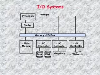
Interrupt Controller The interrupt controller receives interrupt signals from the peripheral modules and external pins Sends interrupts to the CPU, and activates the DTC (Data Transfer Controller)and DMAC (DMA Controller) Performs the following processing: Detecting interrupts Enabling and disabling interrupts Selecting interrupt request destinations (CPU interrupt, DTC activation, or DMAC activation) Determining priority Interrupt requests are detected in either of two ways: The detection of edges of the interrupt signal The detection of a level of the interrupt signal Edge detection or level detection is selected for the IRQi pins (i = 0 to 7) as external interrupt requests By the setting of the IRQMD[1:0] bits in IRQCRi
Interrupt Controller (cont.) For interrupts from peripheral modules, either edge detection or level detection is determined per interrupt source The operation of edge detection of an interrupt The IR flag in IRn is set to 1 immediately after the transition of the interrupt signal due to generation of the interrupt If the CPU is the request destination for the interrupt, the IR flag is automatically cleared to 0 on acceptance of the interrupt If the DMAC or DTC is the request destination for the interrupt, the IRn.IR flag operation differs according to the DMAC/DTC transfer settings and transfer count If an interrupt signal is generated every clock cycle, the subsequent interrupts cannot be detected Secure two or more clock cycles of the system clock or peripheral clock, whichever is slower If an interrupt is disabled after the IRn.IR flag is set to 1, the IRn.IR flag is not affected but retains its state Output of the interrupt request is disabled by the interrupt enable bit of the relevant peripheral module
Interrupt Controller (cont.) The operation of level detection of an interrupt The IR flag in IRn remains set to 1 as long as the interrupt signal is asserted To clear the IRn.IR flag to 0, clear the interrupt request in the source generating the interrupt Confirm that the interrupt request flag in the source generating the interrupt has been cleared to 0 and that the IRn.IR flag has been cleared to 0, and then complete the interrupt handling
Interrupt Controller (cont.) Enabling requests from a given interrupt source requires the following settings: For peripheral modules, setting the interrupt enable bit for the peripheral module to permit interrupt requests from the source Enabling of the interrupt by the IERm.IENj bit When an interrupt request that is enabled at the corresponding source is generated The corresponding IRn.IR flag is set to 1 Setting the IERm.IENj bit to enable an interrupt request allows the interrupt request for which the corresponding IRn.IR is 1 to be output to the interrupt request destination Setting the IERm.IENj bit to disable an interrupt request suspends the output of the interrupt request for which the corresponding IRn.IR is 1 The IRn.IR flag is not affected by the IERm.IENj bit
Interrupt Controller (cont.) Use the following procedure to disable interrupt requests Set the IERm.IENj bit to disable interrupt requests Set the peripheral module interrupt output enable bit to disable the output Read the last written register and confirm that writing is completed Check the IRn.IR flag, and clear the IRn.IR flag if necessary Possible settings for the request destination of each interrupt are fixed Settings for request destination other than those indicated in the Interrupt Vector Table are not possible If the DMAC or DTC is selected as the destination for requests from an IRQ pin Be sure to set the IRQMD[1:0] bits in IRQCRi for that interrupt to select edge detection If the interrupt request destination is neither the DMAC nor the DTC, the interrupt request is sent to the CPU Set the IERm.IENj bit to 1
Interrupt Controller (cont.) Interrupt priority is determined for each interrupt request destination Determining Priority when the CPU is the Request Destination of the Interrupt A source selected for the fast interrupt has the highest priority After that, an interrupt source with a larger value of the interrupt priority level select bits (IPR[3:0]) in IPRn takes priority If interrupts with the same priority level are generated by multiple sources, the source with the smallest vector number is the first Determining Priority when the DTC is the Request Destination of the Interrupt The IPR[3:0] bits in IPRn have no effect An interrupt source with a smaller vector number takes precedence Determining Priority when the DMAC is the Request Destination of the Interrupt The IPR[3:0] bits in IPRn have no effect The order of priority of DMAC channels is based on DMA Controller
Interrupt Controller (cont.) To enable multiple interrupts of the CPU Set the PSW.I bit to 1 (interrupt enabled) in the handling routine of accepted interrupts The PSW.IPL[3:0] bits immediately are set to the same value as the interrupt priority level of the accepted interrupt request If an interrupt request which has an interrupt level higher than that of the PSW.IPL[3:0] bits is generated at this time, this interrupt request is accepted If the interrupt priority level of the accepted interrupt request is 15, multiple interrupts are not generated Fast interrupt or interrupt when IPR[3:0] are set to 1111b The fast interrupt is an interrupt for executing a faster interrupt response by the CPU Only one of the interrupt sources can be assigned The interrupt priority level of the fast interrupt is 15 (highest) The fast interrupt is accepted with precedence over other interrupt sources with level 15
Interrupt Controller (cont.) When the value of the PSW.IPL[3:0] bits are 1111b (priority level 15), even the fast interrupt cannot be accepted To assign an interrupt source to the fast interrupt, specify the vector number of the source in the FIR.FVCT[7:0] bits Set the FIR.FIEN bit to 1 (fast interrupt is enabled) The digital filter function is provided for the external interrupt request IRQi pins (i = 0 to 7) and NMI pin interrupt Samples input signals at the filter sampling clock (PCLK) Removes the pulses of which length is less than three cycles To use the digital filter for the IRQi pin, set the sampling clock cycle (PCLK, PCLK/8, PCLK/32, or PCLK/64) with the IRQFLTC0.FCLKSELi[1:0] bits (i = 0 to 7) Set the IRQFLTE0.FLTENi bit to 1 (digital filter enabled) To use the digital filter for the NMI pin, set the sampling clock cycle (PCLK, PCLK/8, PCLK/32, or PCLK/64) with the NMIFLTC.NFCLKSEL[1:0] bits Set the NMIFLTE.NFLTEN bit to 1 (digital filter enabled)
Interrupt Controller (cont.) The procedure for using the signal on an external pin as an interrupt: Clear the IERm.IENj bit to 0 (interrupt request disabled) Clear the IRQFLTE0.FLTENi bit (i = 0 to 7) to 0 (digital filter disabled) Set the digital filter sampling clock with the IRQFLTC0.FCLKSELi[1:0] bits Make or confirm the I/O port settings Set the method of detection for the interrupt in the IRQCRi.IRQMD[1:0] bits Clear the corresponding IRn.IR flag to 0 If edge detection is in use Set the IRQFLTE0.FLTENi bit to 1 (digital filter enabled) If for DMAC activation, set the DMRSRm.DMRS[7:0] bits If for DTC activation, set the DTCERn.DTCE bit The interrupt will be a CPU interrupt if neither is made
Interrupt Controller (cont.) Set the IERm.IENj bit to 1 (interrupt request enabled) There are six types of non-maskable interrupt: The NMI pin interrupt, oscillation stop detection interrupt, WDT underflow/refresh error, IWDT underflow/refresh error, voltage monitoring 1 interrupt, and voltage monitoring 2 interrupt They are only usable as interrupts for the CPU They are not capable of DTC or DMAC activation Non-maskable interrupts take precedence over all interrupts, including the fast interrupt Non-maskable interrupt requests are accepted regardless of the states of the I (interrupt enable) bit and IPL[3:0] bits in the PSW of the CPU The current states of the non-maskable interrupts can be checked in the non-maskable interrupt status register (NMISR) Confirm that all bits in the NMISR have returned to 0 from within the handler for the non-maskable interrupt Non-maskable interrupts are disabled by default.
Interrupt Controller (cont.) If to use non-maskable interrupts, the following procedure must be followed at the beginning of program processing: Set the stack pointer (SP) To use the NMI pin, clear the NMIFLTE.NFLTEN bit to To use the NMI pin, set the digital filter sampling clock with the NMIFLTC.NFCLKSEL[1:0] bits To use the NMI pin, set the NMI pin detection sense with the NMICR.NMIMD bit To use the NMI pin, write 1 to the NMICLR.NMICLR bit to clear the NMISR.NMIST flag to 0 To use the NMI pin, set the NMIFLTE.NFLTEN bit to 1 (digital filter enabled) Enable the non-maskable interrupt by writing 1 to the right bit in the non-maskable interrupt enable register (NMIER) The NMI interrupt cannot be disabled Can be disabled only by a reset
Interrupt Controller (cont.) Interrupt Request Register n (IRn) (n = interrupt vector no.) Interrupt RequFast Interrupt Set Register (FIR)
Interrupt Controller (cont.) Interrupt Request Enable Register m (IERm)
Interrupt Controller (cont.) Interrupt Source Priority Register n (IPRn) (n = 000 to 250)
Interrupt Controller (cont.) Software Interrupt Activation Register (SWINTR) DTC Activation Enable Register n (DTCERn)
Interrupt Controller (cont.) DMAC Activation Request Select Register m IRQ Control Register i (IRQCRi) (i = 0 to 7)
Interrupt Controller (cont.) IRQ Pin Digital Filter Enable Register 0 (IRQFLTE0)
Interrupt Controller (cont.) IRQ Pin Digital Filter Setting Register 0 (IRQFLTC0)
Interrupt Controller (cont.) Non-Maskable Interrupt Status Register (NMISR)
Interrupt Controller (cont.) Non-Maskable Interrupt Enable Register (NMIER)
Interrupt Controller (cont.) Non-Maskable Interrupt Status Clear Register (NMICLR)
Interrupt Controller (cont.) NMI Pin Digital Filter Enable Register (NMIFLTE) NMI Pin Digital Filter Setting Register (NMIFLTC)
Interrupt Controller (cont.) NMI Pin Interrupt Control Register (NMICR)