Download
1 / 73
740 likes | 876 Views
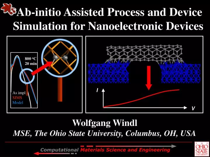
800 o C 20 min. I. As impl. SIMS Model. V. Ab-initio Assisted Process and Device Simulation for Nanoelectronic Devices. Wolfgang Windl MSE, The Ohio State University, Columbus, OH, USA. Semiconductor Devices – MOSFET. Metal Oxide Semiconductor Field Effect Transistor. 0 V G. – V G.

E N D
800 oC 20 min I As impl. SIMS Model V Ab-initio Assisted Process and Device Simulation for Nanoelectronic Devices Wolfgang Windl MSE, The Ohio State University, Columbus, OH, USA
Semiconductor Devices – MOSFET Metal Oxide Semiconductor Field Effect Transistor 0VG – VG – VD – VD Insulator (SiO2) Spacer Gate (Me) Gate ID Source P Drain P Source P Drain P Channel + + + + + + + + + - + + + + + + - - + + + + + + + + + + - - + + + + + + + + - + + + + N + + + - + - + + + + + + N - Si - Si - - - - - - - - - - - - - Doping: N: e-, e.g. As (Donor) P: holes, e.g. B (Acceptor) • Analog: Amplification • Digital: Logic gates
1. Semiconductor Technology Scaling – Improving Traditional TCAD • Feature size shrinks on average by 12% p.a.; speed size • Chip size increases on average by 2.3% p.a. • Overall performance: by ~55% p.a. or • ~ doubling every 18 months (“Moore’s Law”)
Semiconductor Technology Scaling – Gate Oxide Bacterium 0VG – VD Gate oxide (SiO2) Gate (Me) Virus Source P Drain P Channel + + + + - + + + - - + + + + + - + + + + + + - N + + Proteinmolecule + + + - Si - - - - - - Atom C = A/d
Improving traditional (continuum) process modeling to include nanoscale effects Identify relevant equations & parameters (“physics”) Basis for atomistic process modeling (Monte Carlo, MD) Nanoscale characterization = Combinationof experiment & ab-initio calculations Atomic-level process + transport modeling = structure-property relationship (“ultimate goal”) Role of Ab-Initio Methods on Nanoscale
1. “Nanoscale” Problems – Traditional MOS • What you get: • fast diffusion (TED) • immobile peak • segregation Active B¯ 800 °C 20 min What you expect: Intrinsic diffusion 800 °C 20 min 800 °C 1 month
Bridging the Length Scales: Ab-Initio to Continuum Need to calculate: ● Diffusion prefactors (Uberuaga et al., phys. stat. sol. 02) ● Migration barriers (Windl et al., PRL 99) ● Capture radii (Beardmore et al., Proc. ICCN 02) ●Binding energies (Liu et al., APL 00)
Traditional characterization techniques, e.g.: SIMS (average dopant distribution) TEM (interface quality; atomic-column information) Missing: “Single-atom” information Exact interface (contact) structure (previous; next) Atom-by-atom dopant distribution (strong VT shifts) New approach: atomic-scale characterization (TEM) plus modeling 2. The Nanoscale Characterization Problem
Abrupt vs. Diffuse Interface Abrupt Graded Si0 Si0 Si2+ Si1,2,3+ Si4+ Si4+ How do we know? What does it mean? Buczko et al.
Atomic Resolution Z-Contrast Imaging < 0.1 nm Scanning Probe Z=31 Z=33 GaAs A n n u l a r D e t e c t o r As Ga 1.4Å EELS Spectrometer Computational Materials Science and Engineering
CB x25 x500 x5000 optical properties and electronic structure VB C-K Si-L bonding and oxidation state concentration O-K Core hole Z+1 100 200 300 400 500 LOSS CORE VALENCE LOSS Electron Energy-Loss Spectrum 70 silicon with surface oxide and carbon contamination 60 intensity (a.u.) 50 40 30 20 10 0 0 ZERO energy loss (eV) LOSS
Theoretical Methods ab initio Density Functional Theory plus LDA or GGA implemented within pseudopotential and full-potential (all electron) methods
Si-L2,3 Ionization Edge in EELS ground state of Si atom with total energy E0 excited Si atom with total energy E1 energy conduction band minimum EF ~ 90eV ~ 115eV site and momentum resolved DOS 2p6 2p3/2 2p1/2 2p5 2s1/2 Transition energy ET = E1 - E0 ET = ~100 eV 1s1/2
Calculated Si-L2,3 Edges at Si/SiO2 Si 0.8 0.4 0 Si3+ 0.6 Si1+ 0.2 1.2 Si2+ 0.4 0 Si4+ 1 0.5 0 108 104 100 Energy-loss, eV
Combining Theory and Experiment Calculation of EELS Spectra from Band Structure Si - L2,3 Si Intensity 0.5 nm 100 105 110 Energy-loss (eV)
Combining Theory and Experiment Fractions .74 4 3 2 1 Si0 Si1+ Si2+ Si3+ Si4+ Calculation of EELS Spectra from Band Structure Si - L2,3 Si Intensity 0.5 nm 100 105 110 Energy-loss (eV) “Measure” atomic structure of amorphous materials.
Band Line-Up Si/SiO2 • Real-space band structure: • Calculate electron DOS projected on atoms • Average layers • Abrupt would be better! Is there an abrupt interface? Lopatin et al., submitted to PRL
Initial Ge distribution Interfaces with Different Abruptness:Si/SiO2 vs. Si:Ge/SiO2 • Yes! • Ge-implanted sample from ORNL (1989). • Sample history: • Ge implanted into Si (1016 cm-2, 100 keV) • ~ 800 oC oxidation ~4% ~120 nm
peak ~100% Ge Intensity SiO2 Ge Si 1 2 3 4 5 6 nm Z-Contrast Ge/SiO2 Interface • Ge after oxidation packed into compact layer,~ 4-5 nm wide
Simulation Algorithm for oxidation of Si:Ge: Si lattice with O added between Si atoms Addition of O atoms and hopping of Ge positions by KMC* First-principles calculation of simplified energy expression as function of bonds: Kinetic Monte Carlo Ox. Modeling • *Hopping rate Ge: McVay, PRB 9 (74); ox rate SiGe: Paine, JAP 70 (91). Windl et al., J. Comput. Theor. Nanosci.
Monte Carlo Results - Animation Ge conc. O conc. Concentration (cm-3) • O • Ge • Si not shown • 2422 nm3 Depth (cm)
Initial Ge distribution 25 min, 1000 oC Monte Carlo Results - Profiles oxide
oxide SiGe Si/SiO2 vs. Ge/SiO2 Atomic Resolution EELS Intensity Si - L2,3 Ge Si - L2,3 Si Intensity 0.5 nm 0.5 nm 100 105 110 100 105 110 Energy-loss (eV) Energy-loss (eV) S. Lopatin et al., Microscopy and Microanalysis, San Antonio, 2003.
Band Line-Up Si/SiO2 & Ge/SiO2 Lopatin et al., submitted to PRL
Conclusions 2 • Atomic-scale characterization is possible: Ab-initio methods in conjunction with Z-contrast & EELS can resolve interface structure. • Atomically sharp Ge/SiO2 interface observed • Reliable structure-property relationship for well characterized structure (band line-up) • Abrupt is good • Sharp interface from Ge-O repulsion (“snowplowing”)
3. Process and Device Simulation of Molecular Devices • Possibilities: • Carbon nanotubes (CNTs) as channels in field effect transistors • Single molecules to function as devices • Molecular wires to connect device molecules • Single-molecule circuits where devices and interconnects are integrated into one large molecule 300 nm Wind et al., JVST B, 2002.
Concept of Ab-Initio Device Simulation device • Using • Landauer formula for Ip(V) • Lippmann-Schwinger equation, Tlr(E) = lV + VGV r • Rigid-band approximation T(E,V) = T(E + V) with = 0.5 Zhang, Fonseca, Demkov,Phys Stat Sol (b), 233, 70 (2002)
left elec. (Hl) device (Hd) right elec. (Hr) ... ... Tdr Tr Tdl Tl Tlr from Local-Orbital Hamiltonian • Tlr(E) can be constructed from matrix elements of DFT tight-binding Hamiltonian H. Pseudo atomic orbitals: (r > rc)=0. • We use matrix-element output from SIESTA. Zhang, Fonseca, Demkov,Phys Stat Sol (b), 233, 70 (2002)
The Molecular Transport Problem I Expt. • Strong discrepancy expt.-theory! • Suspected Problems: • Contact formation molecule/lead not understood • Influence of contact structure on electronic properties Theor.
What is “Process Modeling” for Molecular Devices? s ms Moore’s law ms ns 1990 2000 2010 Year • Contact formation: need to follow influence of temperature etc. on evolution of contact. • Molecular level: atom by atom Molecular Dynamics • Problem:MD may never get to relevant time scales Accessible simulated time* * 1-week simulation of 1000-atom metal system, EAM potential
Accelerated Molecular Dynamics Methods • Possible solution: accelerated dynamics methods. • Principle: run for trun. Simulated time: tsim = ntrun, n >> 1 • Possible methods: • Hyperdynamics (1997) • Parallel Replica Dynamics (1998) • Temperature Accelerated Dynamics (2000) Voter et al., Annu. Rev. Mater. Res. 32, 321 (2002).
Temperature Accelerated Dynamics (TAD) • Concept: • Raise temperature of system to make events occur more frequently. Run several (many) times. • Pick randomly event that should have occurred first at the lower temperature. • Basic assumption (among others): • Harmonic transition state theory (Arrhenius behavior) w/E from Nudged Elastic Band Method (see above). Voter et al., Annu. Rev. Mater. Res. 32, 321 (2002).
Carbon Nanotube on Pt • From work function, Pt possible lead candidate. • Structure relaxed with VASP. • Very small relaxations of Pt suggest little wetting between CNT and Pt ( bad contact!?).
Movie: Carbon Nanotube on PtTemperature-Accelerated MD at 300 K tsim = 200 s • Nordlund empirical potential • Not much interaction observed study different system.
Carbon Nanotube on Ti • Large relaxations of Ti suggest strong reaction (wetting) between CNT and Ti. • Run ab-initio TAD for CNT on Ti (no empirical potential available). • Very strong reconstruction of contacts observed.
TAD MD for CNT/Ti 600 K, 0.8 pstsim (300 K) = 0.25 s CNT bonds break on top of Ti, very different contact structure. New structure 10 eV lower in energy.
Contact Dependence ofI-V Curve for CNT on Ti Difference 15-20%
Relaxed CNT on Ti “Inline Structure” • In real devices, CNT embedded into contact. Maybe major conduction through ends of CNT?
Contact Dependence ofI-V Curve for CNT on Ti Inline structure has 10x conductivity of on-top structure
Conclusions • Currently major challenge for molecular devices: contacts • Contact formation: “Process” modeling on MD basis. • Accelerated MD • Empirical potentials instead of ab initio when possible • Major pathways of current flow through ends of CNT
Funding • Semiconductor Research Corporation • NSF-Europe • Ohio Supercomputer Center
Acknowledgments (order of appearance) • Dr. Roland Stumpf (SNL; B diffusion) • Dr. Marius Bunea and Prof. Scott Dunham (B diffusion) • Dr. Xiang-Yang Liu (Motorola/RPI; BICs) • Dr. Leonardo Fonseca (Freescale; CNT transport) • Karthik Ravichandran (OSU; CNT/Ti) • Dr. Blas Uberuaga (LANL; CNT/Pt-TAD) • Prof. Gerd Duscher (NCSU; TEM) • Tao Liang (OSU; Ge/SiO2) • Sergei Lopatin (NCSU; TEM)
Left: • Ti below 25 a.u. and above 55 a.u. • CNT (armchair (3,3), 12 C planes) in the middle • Right: • Ti below 10 a.u. and above 60 a.u. • CNT (3,3), 19 C planes, in contact with Ti between 15 a.u. and 30 a.u. and between 45 a.u. and 60 a.u. • CNT on vacuum between 30 a.u. and 45 a.u.
Minimal basis set used (SZ); I did a separate calculation for an isolated CNT(3,3) and obtained a band gap of 1.76 eV (SZ) and 1.49 eV (DZP). Armchair CNTs are metallic; to close the gap we need kpts in the z-direction.
Notice the difference in the y-axis. The X structure (below) carries a current which is about one order of magnitude smaller than the CNT inline with the contacts (left) The main peak in the X structure is located at ~5 V, which is close to the value from the inline structure (~5.5 V). This indicates that the qualitative features in the conductance derive from the CNT while the magnitude of the conductance is set by the contacts. The extra peaks seen on the right may be due to incomplete relaxation.
Notice the difference in the y-axis. The X structure (below) carries a current which is about one order of magnitude smaller than the CNT inline with the contacts (left) The main peak in the X structure is located at ~5 V, which is close to the value from the inline structure (~5.5 V). This indicates that the qualitative features in the conductance derive from the CNT while the magnitude of the conductance is set by the contacts. The extra peaks seen on the right may be due to incomplete relaxation.
PDOS for the relaxed CNT in line with contacts. The two curves correspond to projections on atoms far away from the two interfaces. A (3,3) CNT is metallic, still there is a gap of about 4 eV. Does the gap above result from interactions with the slabs or from lack of kpts along z? This question is not so important since the Fermi level is deep into the CNT valence band.
Previous calculations and new ones. Black is unrelaxed but converged with Siesta while blue is relaxed with Vasp and converged with Siesta. From your results it looks like you started from an unrelaxed structure and is trying to converge it.
Current (A) Bias (V) Previous calculations and new ones. Black is relaxed with Vasp and converged with Siesta.