Download
1 / 58
670 likes | 915 Views
SOI Technology: Overview and Device Physics. Jean-Pierre Colinge University of California Davis, CA, USA. Outline. ◊ Introduction (Where SOI Technology stands today) ◊ SOI Materials (SOS, SIMOX, Wafer Bonding, Unibond ® ) ◊ The “Classical” SOI MOSFET (Partially/Fully Depleted)

E N D
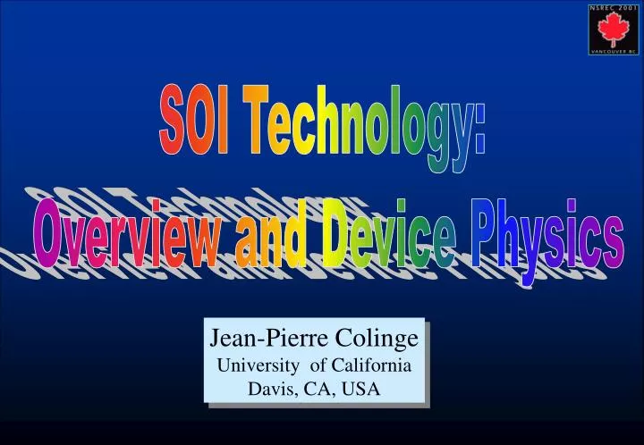
SOI Technology: Overview and Device Physics Jean-Pierre Colinge University of California Davis, CA, USA
Outline ◊ Introduction (Where SOI Technology stands today) ◊ SOI Materials (SOS, SIMOX, Wafer Bonding, Unibond®) ◊ The “Classical” SOI MOSFET (Partially/Fully Depleted) ◊ Other SOI MOSFETs (Hybrid, Double Gate, Ground Plane, multiple gates) ◊ SOI Circuits (Hi-T°, Low-Power, RAMs)
Outline ◊ Introduction (Where SOI Technology stands today) ◊ SOI Materials (SOS, SIMOX, Wafer Bonding, Unibond®) ◊ The “Classical” SOI MOSFET (Partially/Fully Depleted) ◊ Other SOI MOSFETs (Hybrid, Double Gate, Ground Plane, multiple gates) ◊ SOI Circuits (Hi-T°, Low-Power, RAMs)
US Semiconductor Manufacturers Using SOI IBM PD Microprocessor Motorola PD/FD Microprocessor AMD PD/FD Microprocessor TI PD Various HP PD Microprocessor Peregrine FD (SOS) RF, logic, EEPROM analog, Rad-hard Synova PD Rad-Hard Honeywell PD Hi-T°; Rad-hard Lincoln Lab FD Low-power, Rad-hard SOI news web site: http://www.soisolutions.com
Advertisement page in USA Today, in Oct. 2000: IBM uses SOI and copper for its top-of-line servers
G5 * 0.1 mm process with initial G5 product * 2 GHz G4 * 0.15 mm copper process for initial G4 product (migrating to 1 GHz) * up to 1 GHz
Motorola IBM Power PC Honeywell CLEARWATER, FLA. FEBRUARY 4, 1999 - Honeywell Space Systems and Motorola Semiconductor Products Sector today announced a joint licensing agreement for PowerPC* technology for use in Honeywell space processors. The result will be a next generation space microprocessor which will be radiation hardened to withstand the destructive effects of space, will operate with Power PC software and use less power. Internally, Honeywell is referring to this next generation microprocessor as the Space Processor Chip (SpacePC). It combines the capabilities of the advanced Motorola PowerPC 603e microprocessor with Honeywell’s radiation and performance enhancing Silicon On Insulator (SOI) technology.
Outline ◊ Introduction (Where SOI Technology stands today) ◊ SOI Materials (SOS, SIMOX, Wafer Bonding, Unibond®) ◊ The “Classical” SOI MOSFET (Partially/Fully Depleted) ◊ Other SOI MOSFETs (Hybrid, Double Gate, Ground Plane, multiple gates) ◊ SOI Circuits (Hi-T°, Low-Power, RAMs)
SIMOX Silicon Silicon SIMOX, circa 1985 SIMOX, 1998 BOX BOX 1,000,000,000 dislocations/cm2 3,000 dislocations/cm2
Outline ◊ Introduction (Where SOI Technology stands today) ◊ SOI Materials (SOS, SIMOX, Wafer Bonding, Unibond®) ◊ The “Classical” SOI MOSFET (Partially/Fully Depleted) ◊ Other SOI MOSFETs (Hybrid, Double Gate, Ground Plane, multiple gates) ◊ SOI Circuits (Hi-T°, Low-Power, RAMs)
MOSFETs Gate Oxide Gate Partially Depleted SOI + + N Source N Drain Depletion zone 0.1-0.2 µm Buried oxide P- type silicon Bulk Fully Depleted SOI
Source and Drain Capacitance -7 10 17 -3 Bulk, N =10 cm B + SOI, P drain on P-substrate, 15 -3 t =400 nm, N =10 cm -8 BOX B 10 Drain capacitance (F/cm2) + SOI, N drain on P-substrate, 15 -3 t =400 nm, N =10 cm BOX B -9 10 0 1 2 3 4 5 Supply voltage (V)
SOI MOSFET: a few definitions V g1 V ds Gate t ox1 + + FD: 30-80 nm PD:100-200 nm P Source (N ) Drain (N ) t s i t ox2 60-400 nm Buried oxide Back gate (mechanical substrate) V g2
Possible Edge Leakage Field Isolation LOCOS Mesa STI
Edge Leakage Elimination And Body Ties A: Regular SOI MOSFET; B: Edgeless device Body ties in source A: Lateral body tie; B: H-gate body tie
SOI MOSFET: DIBL or: Drain-Induced Barrier Lowering Electric field lines from the drain encroach on the channel region. Any increase of drain voltage decreases the threshold voltage (the “NPN” potential barrier between source and drain is lowered). E-field lines
SOI MOSFET PDSOI MOSFET FDSOI MOSFET Pro: better VTH control Con: floating substrate effects Remedy: Body tie Pro: better electrical properties Con: worse VTH control* Remedy: Uniform SOI material OFFSPRING OFFSPRING Hybrid (DTMOS, MTCMOS) Double gate Multiple gate Buried ground plane electrode * s VTH < 9 mV in literature
PDSOI MOSFET Front Gate Source Drain Back Gate
PDSOI MOSFET: Kink Effect Front Gate 1. Impact ionization 2. Hole injection in floating substrate 3. Forward bias diode 4. Increase of floating body potential 5. Reduces VTH 6. Increases current 1 2 Source Drain 3 4 Back Gate
PDSOI MOSFET: Kink Effect Current is increased (GOOD!) Output conductance (or Early voltage) is very poor (BAD!) Drain Current Drain Voltage
SOI MOSFET: Single-Transistor Latchup Front Gate Source Drain Back Gate Illustration of the single-transistor latch. "Normal" subthreshold slope at low drain voltage (a), infinite subthreshold slope and hysteresis (b), and device "latch-up" (c).
PDSOI MOSFET: floating-body effects Front Gate 250 ms VG Source Drain ID Floating body 20 ms VG Back Gate ID This is only one example among MANY!
MOSFET Equations: Body Factor Non saturation: Saturation: Subthreshold swing: Gain (weak inversion): Gain (strong inversion):
Gate - Channel Coupling Body factor: n = …1.5… in Bulk; n = …1.05... in FDSOI
-6 -7 -8 -9 -10 -11 -12
Microwave SOI MOSFETs Noise figure / f f SOI L V I T max D D Associated gain material (µm) (GHz) (GHz) (dB) at 2GHz (V) (mA) BESOI 1 - - - 14 5 / 6.4 SIMOX 1 - - - 11 5 / 4.4 SOS 0.35 3 10 23 56 - / - SIMOX 0.32 3 33 14 21 3 / 13.4 SIMOX 0.25 3 41 23.6 32 1.5 / 17.5 SIMOX 0.75 0.9 3 10 11 1.5 / 9 SIMOX 0.75 0.9 10 12.9 30 - / 13.9 (10.4¥) SIMOX 0.3 2 - - 24.3 0.9 / 14 SOS* 0.5 2 2 26 60 1.7 / 16.3 SIMOX 0.2 2 125 28.4 46 1/15.3 † SIMOX 0.07 1.5 5 150 Unibond 0.25 1.5 50 75 (*) Metal-gate technology is used; (†) at 3 GHz and (¥) at 5 GHz.
Outline ◊ Introduction (Where SOI Technology stands today) ◊ SOI Materials (SOS, SIMOX, Wafer Bonding, Unibond®) ◊ The “Classical” SOI MOSFET (Partially/Fully Depleted) ◊ Other SOI MOSFETs (Hybrid, Double Gate, Ground Plane, multiple gates) ◊ SOI Circuits (Hi-T°, Low-Power, RAMs)
Hybrid bipolar-MOS aka DTMOS (Dual-Threshold MOS) aka MTCMOS (Multiple-Threshold CMOS)
Leff,N = 0.45 mm, Leff,P = 0.58 mm (1987) Leff,N = Leff,P = 0.3 mm (1994)
Double-Gate SOI MOSFET: Volume Inversion
20°C P-channel N-channel 300°C 300°C 200°C 200°C W = L = 3µm
Ground Plane SOI MOSFET E-field lines E-field lines "The ground-plane concept for the reduction of short-channel effects in fully depleted SOI devices", Ernst, T., and Cristoloveanu, S., Electrochemical Society Proceedings 99-3, p. 329, 1999
Ground-Plane SOI MOSFET P+ implanted ground plane (in Si wafer)
Ground-Plane SOI MOSFET Equipotentials (Regular SOI MOSFET) Equipotentials (Ground-Plane SOI MOSFET)
Regular FD SOI vs. Ground-Plane FD SOI Regular SOI MOSFET Regular SOI MOSFET Ground-Plane SOI MOSFET Ground-Plane SOI MOSFET
Double-Gate SOI MOSFET E-field lines E-field lines J.P. Colinge, M.H. Gao, A. Romano, H. Maes and C. Claeys, Technical Digest of IEDM, p. 595, 1990
Multiple-Gate SOI MOSFETsc Different gate configurations for SOI devices: 1) single gate; 2) double gate; 3) triple gate; 4) quadruple gate (or: gate-all-around structure); 5) ∏-gate MOSFET.
Multiple-Gate SOI MOSFETsc G a t e l e n g t h ( n m ) DIBL in fully depleted SOI MOSFETs with different gate structures and different effective gate lengths. VDS = 100 mV.
Outline ◊ Introduction (Where SOI Technology stands today) ◊ SOI Materials (SOS, SIMOX, Wafer Bonding, Unibond®) ◊ The “Classical” SOI MOSFET (Partially/Fully Depleted) ◊ Other SOI MOSFETs (Hybrid, Double Gate, Ground Plane, multiple gates) ◊ SOI Circuits (Hi-T°, Low-Power, RAMs)