Download
1 / 30
300 likes | 440 Views
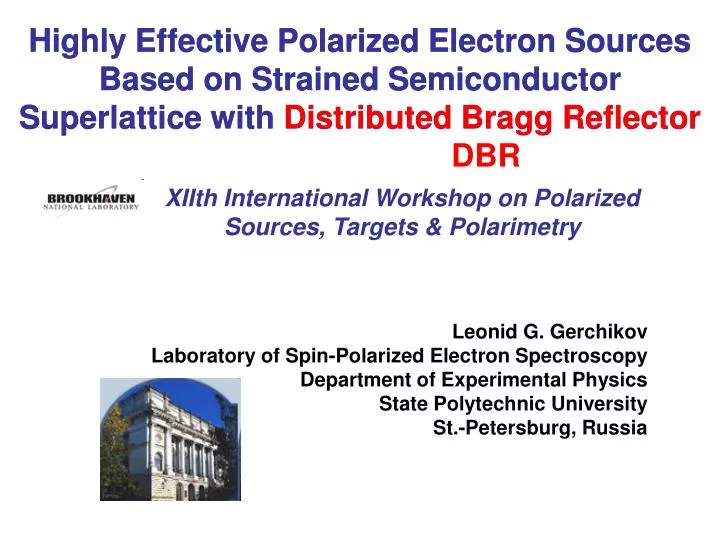
Highly Effective Polarized Electron Sources Based on Strained Semiconductor Superlattice with Distributed Bragg Reflector. Highly Effective Polarized Electron Sources Based on Strained Semiconductor Superlattice with Distributed Bragg Reflector. DBR.

E N D
Highly Effective Polarized Electron Sources Based on Strained Semiconductor Superlattice with Distributed Bragg Reflector Highly Effective Polarized Electron Sources Based on Strained Semiconductor Superlattice with Distributed Bragg Reflector DBR XIIth International Workshop on Polarized Sources, Targets & Polarimetry Leonid G. Gerchikov Laboratory of Spin-Polarized Electron Spectroscopy Department of Experimental Physics State Polytechnic University St.-Petersburg, Russia
Collaborators Department of Experimental Physics, St.Petersburg State Polytechnic University, Russia, Yurii A. Mamaev, Yurii P.Yashin, Vitaly V. Kuz’michev, Dmitry A. Vasiliev, Leonid G. Gerchikov Stanford Linear Accelerator Center, Stanford, CA, USA, James E. Clendenin , Takashi Maruyama A.F. Ioffe Physicotechnical Institute RAS, Russia, Viktor M. Ustinov, Aleksey E. Zhukov, Vladimir S. Mikhrin, Alexey P. Vasiliev Department of Electronic and Electrical Engineering, University of Sheffield, UK, John S. Roberts Institute of Nuclear Physics, Mainz University, Mainz, Germany,Kurt Aulenbacher
OUTLINE • Introduction • High-Energy spin physics requirements • Photocathodes based on strained semiconductor superlattices • Optical resonator with DBR • Design of photocathode • Strain-compensated superlattice photocathode with DBR • Superlattice with strained QW and DBR • Summary & Outlook
High-Energy physics requirements 90% is better • High electron polarization, P > 80% • High QE for large beam currents • Large electronic current requirement • Light energy limitations: • Surface charge saturation • Heating High QE
High polarization of electron emission from strained semiconductor SL at the expense of QE Spectra of electron emission:Polarization P and Quantum Efficiency QE SL Al0.2 In0.155 Ga0.65As(5.1nm)/Al0.36Ga0.64As(2.3nm) • Polarization is maximal at photoabsorption threshold where QE is small. • Strain relaxation does not allow to produce thick photocathode with high QE. • Rise of the vacuum level increases P and decreases QE
Goal: considerable increase of QE at the main polarization maximum.Method: Resonance enhancement of photoabsorption in SL integrated into Fabry-Perot optical cavity. Photoabsorption in the working layer: L 1, - photoabsorbtion coefficient, L - thickness of SL Resonant enhancement by factor 2/(1-(RDBRRGaAs) 1/2)2
Resonant enhancement of polarized electron emission from strained semiconductor layer T. Saka, T.Kato, T.Nakanishi, M.Tsubata, K.Kishino, H.Horinaka, Y.Kamiya, S.Okumi, C.Takahashi, Y.Tanimoto, M.Tawada, K.Togawa, H.Aoyagi, S.Nakamura, Jpn. J. Appl. Phys. 32, L1837 (1993).
Resonant enhancement of polarized electron emission from strained semiconductor layer J. C. Groebli, D. Oberli, F. Meier, A. Dommann, Yu. Mamaev, A. Subashiev and Yu. Yashin, Phys. Rev. Lett. 74, 2106 (1995).
Optimization of Photocathode structure • SL structure: layers composition and thickness are chosen to assure • Eg= for P()=Pmax • Ehh-lh > 60meV for high polarization • Ee1 > 40meV for effective electron transport • DBR structure: 20x(AlAs(/4)/ (AlxGa1-xAs(/4)) • Layer thickness l = /4n() for Bragg reflection • x 0.8 for large reflection band width = 2n/n • Fabry-Perot resonance cavity: BBR + SL + buffer layer • Effective thickness = k /2 for QE() = QEmax • Effective thickness of BBR+SL /4
Simulation of resonant photoabsorption • SL’s energy band structure, photoabsorption coefficient, polarization of photoelectrons. Method: kp – method within 8-band Kane model. A.V. Subashiev, L.G. Gerchikov, and A.I. Ipatov. J. Appl. Phys., 96, 1511 (2004). • Distribution of electromagnetic field in resonance cavity, reflectivity, QE. Method: transfer matrixes. M.Born and E.Wolf. Princeples of Optics, Pergamon Press, New York, 1991
Problems of fabrications • Even small in-plane anisotropy leads to resonant polarization losses. High quality structure of Fabry-Perot cavity is required. • The optical thickness of Fabry-Perot cavity can not be adjusted after fabrication.
Strain-compensated SL GaAs BBR Tensiled barrier ab < a0 Stressed QW aw > a0 SL Stressed QW aw > a0 Tensiled barrier ab < a0 Buffer Layer a0 - latt. const DBR GaAs Substrate • Features: • No strain relaxation • Thick working layer without structural defects • Large deformation splitting in each SL layer
MOVPE grown AlInGaAs-GaAsP strained-compensated SLs “Resonance Enhancement of Spin-Polarized Electron Emission from Strain Compensated AlInGaAs GaAsP Superlattices” J.S. Roberts, Yu.P. Yashin, Yu. A. Mamaev, L.G.Gerchikov,T. Maruyama, D.-A. Luh, J.E. Clendenin, Proceedings of the 14th international conference “Nanostructures: Physics and Technology”, St.Petersburg, 26-30 June 2006.
Reflectivity Theory , QT 1890 DBR Experiment, QT 1890 DBR
Strained-well SL GaAs BBR Strained QW aw > a0 SL Strained QW aw > a0 Unstrained barrier ab = a0 Buffer Layer a0 - latt. const DBR GaAs Substrate Unstrained barrier ab = a0 • Feature: • Large valence band splitting due to combination of deformation and quantum confinement effects in QW
MBE grown AlInGaAs/AlGaAs strained-well superlattice SPTU & FTI, St.Petersburg, 2006
Summary & Outlook • We have developed a novel type photocathode based on strain compensated superlattices integrated into a Fabry-Perot optical cavity of high structural quality. • We demonstrate a tenfold enhancement of quantum efficiency without polarization losses due to the multiple resonance reflection from DBR layer. • The obtained results demonstrate the advantages of the developed photocathode as a perspective candidate for spin polarized electron sources.
Acknowledgments This work was supported by • Russian Ministry of Education and Science under grant N.P. 2.1.1.2215 in the frames of a program “Development of the High School scientific potential” • Swiss National Science Foundation under grant SNSF IB7420-111116