Download
1 / 23
360 likes | 813 Views
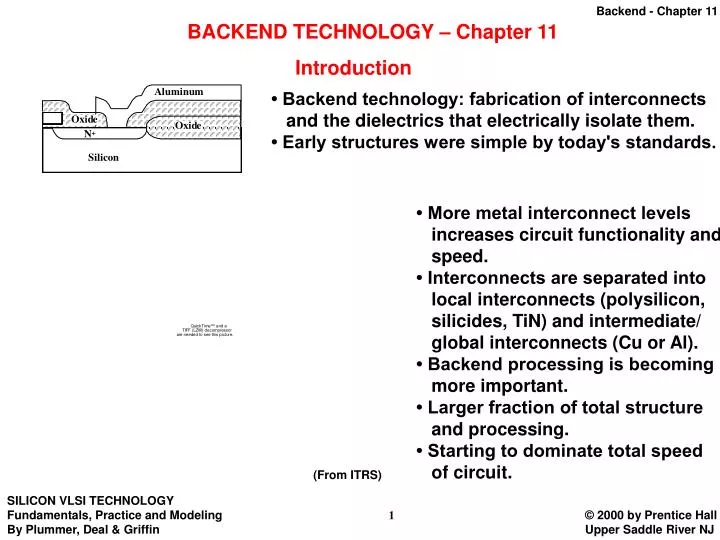
BACKEND TECHNOLOGY – Chapter 11. Introduction. • Backend technology: fabrication of interconnects and the dielectrics that electrically isolate them. • Early structures were simple by today's standards. • More metal interconnect levels increases circuit functionality and

E N D
BACKEND TECHNOLOGY – Chapter 11 Introduction • Backend technology: fabrication of interconnects and the dielectrics that electrically isolate them. • Early structures were simple by today's standards. • More metal interconnect levels increases circuit functionality and speed. • Interconnects are separated into local interconnects (polysilicon, silicides, TiN) and intermediate/ global interconnects (Cu or Al). • Backend processing is becoming more important. • Larger fraction of total structure and processing. • Starting to dominate total speed of circuit. (From ITRS)
• The speed limitations of interconnects can be estimated fairly simply. • The time delay (rise time) due to global interconnects is: (1) where Kox is the dielectric constant of the oxide, KI accounts for fringing fields and is the resistivity of the interconnect line. • Simple analysis of interconnect and gate time delay versus chip area.
• More sophisticated analysis from the 2003 ITRS interconnect roadmap. • Global interconnects dominate the RC delays. • “In the long term, new design or technology solutions (such as co-planar waveguides, free space RF, optical interconnect) will be needed to overcome the performance limitations of traditional interconnect.” (ITRS) Historical Development and Basic Concepts A. Contacts • Early structures were simple Al/Si contacts. • Highly doped silicon regions are necessary to insure ohmic, low resistance contacts. (2) • Tunneling current through a Schottky barrier depends on the width of the barrier and hence ND. • In practice, ND, NA > 1020 are required.
• Another practical issue is that Si is soluble in Al (≈ 0.5% at 450˚C). This can lead to "spiking" problems. • Si diffuses into Al, voids form, Al fills voids shorts! • 1st solution - add 1-2% Si in Al to satisfy solubility. Widely used, but Si can precipitate when cooling down and increase c. • Better solution: use barrier layer(s). Ti or TiSi2 for good contact and adhesion, TiN for barrier. (See Table 11.3 in text for various barrier options.)
B. Interconnects And Vias • • Al has historically been the dominant material for interconnects. • - low resistivity • - adheres well to Si and SiO2 • - can reduce other oxides • - can be etched and deposited easily • • Problems: -relatively low melting point and soft. • need a higher melting point material for gate electrode and local • interconnect polysilicon. • - hillocks and voids easily formed in Al. • Hillocks and voids form because of stress and diffusion in Al films. Heating places Al under compression causing hillocks. Cooling back down can place Al under tension voids. • Adding a few % Cu stabilizes grain boundaries and minimizes hillock formation.
• A related problem with Al interconnects is “electromigration.” High current density (0.1-0.5 MA/cm2) causes movement of Al atoms in direction of electron flow. • Can cause hillocks and voids, leading to shorts or opens in the circuit. • Adding Cu (0.5-4 weight %) can also inhibit electromigration. • Thus Al is commonly deposited with 1-2 wt % Si and 0.5-4 wt % Cu. • Next development was use of other materials with lower resistivity as local interconnects, like TiN and silicides. • Silicides used to 1. strap polysilicon, 2. Strap junctions, 3. as a local interconnect.
• Self-aligned silicide (“salicide”) process. • Also, recall TiN, TiSi2 simultaneous formation in CMOS process in Chapter 2. • Early two-level metal structure (early 1980’s). Non-planar topography leads to lithography, deposition, filling issues. • These issues get worse with additional levels of interconnect and required a change in structure. need to planarize.
Degree of planarization is (3) • One early approach to planarization incorporated W plugs and a simple etchback process. (Damascene process.) • SPEEDIE simulation below.
• More advanced version of the damascene process provides both the via/contact and interconnect levels simultaneously. • In this “dual damascene” process, both the openings in the IMD for the metal interconnect and for the contact or vias underneath are opened, one after the other. • Metal is then deposited into both layers at once followed by a CMP etchback. • Interconnects have also become multilayer structures. • Shunting the Al helps mitigate electromigration and can provide mechanical strength, better adhesion and barriers in multi-level structures. TiN on top also acts as antireflection coating for lithography.
• The biggest change that has occurred in the past 5 years is the widespread introduction of Cu, replacing aluminum. • Cu cannot be easily etched since the byproducts, copper halides are not volatile at room temperature. • Electroplating (see text section 9.3.10) plus a damascene process (single or dual) is the obvious solution and is widely used today. • Cu is the dominant material in logic chips today (µp, ASICs), but not in most memory chips. • Typical modern interconnect structure incorporating all these new features.
C. Dielectrics • Dielectrics electrically and physically separate interconnects from each other and from active regions. • Two types: - First level dielectric - Intermetal dielectric (IMD) • First level dielectric is usually SiO2 “doped” with P or B or both (2-8 wt. %) to enhance reflow properties. • PSG: phosphosilicate glass, reflows at 950-1100˚C • BPSG: borophosphosilicate glass, reflows at 800˚C. • SEM shows BPSG oxide layer after 800˚C reflow step, showing smooth topography over step. • Undoped SiO2 often used above and below PSG or BPSG to prevent corrosion of Al .
• Intermetal dielectrics also made primarily of SiO2 today, but cannot do reflow or densification anneals on pure SiO2 because of T limitations. • Two common problems occur, cusping and voids, which can be minimized using appropriate deposition techniques. • SPEEDIE simulations of silicon dioxide depositions over a step for silane deposition (Sc = 0.4) and TEOS deposition (Sc = 0.1) showing less cusping in the latter case. • However planarization is also usually required today.
• One simple process involves planarizing with photoresist and then etching back with no selectivity. • Spin-on-glass (SOG) is another option: • Fills like liquid photoresist, but becomes SiO2 after bake and cure. • Done with or without etchback (with etchback to prevent poisoned via - no SOG contact with metal). • Can also use low-K SOD’s. (spin-on-dielectrics) • SOG oxides not as good quality as thermal or CVD oxides • Use sandwich layers. • A final deposition option is HDPCVD (see chapter 9) which provides angle dependent sputtering during deposition which helps to planarize. without etchback with etchback
• The most common solution today is CMP which works very well. • It is capable of forming very flat surfaces as shown in the example below.
• Backend structure showing one possible dielectric multi-structure scheme. Other variations include HDP oxide or the use of CMP. • Two backend structures. Left: three metal levels and encapsulated BPSG for the first level dielectric; SOG (encapsulated top and bottom with PECVD oxide) and CMP in the intermetal dielectrics. The multilayer metal layers and W plugs are also clearly seen. Right: five metal levels, HDP oxide (with PECVD oxide on top) and CMP in the intermetal dielectrics.
Models and Simulation • Backend process simulation obviously relies heavily on the deposition and etching simulation tools discussed in Chapters 9 and 10. • We will briefly consider here some additional simulation tools which are useful - starting with REFLOW. • Reflow occurs to minimize the total energy of the system. In this case, the surface energy of the structure is reduced by minimizing the curvature. • Surface diffusion is one reflow mechanism (metals at high T). • Atoms will move to regions of lower chemical potential, µ, which is a (4) function of the curvature. where is the per-area surface energy, is the atomic volume of the atom, K is the curvature, and s is the length along the surface. • The curvature, K, is equal to the inverse of (5) the radius of curvature, R, at that point:
• The force acting upon an atom is in the direction away from a point of higher curvature to a point of lower curvature. A smoothing of the topography results. • The surface flux of atoms, Fs then equals: where is the number of atoms per unit area, and Ds is the surface diffusivity of the atoms. (6) • Simulations of R. Brain, for reflow of Cu at 800K for different trench sizes: a. 1 x 1 µm; b. 0.5 x 1 µm; c. 0.33 x 1 µm; and d. three 0.5 x 1 µm trenches spaced 0.5 µm apart. (parameters given in Table 11.8 in text.) • Note filling of trenches and smoothing of topgraphy.
• Some front-end models have also been applied to back-end processing. • Silicide formation is often modeling using the Deal-Grove linear-parabolic model. (7) • Simulation of TiSi2 formation using FLOOPS [11.32] on a 0.35 m wide gate structure. Left: before formation anneal step. Right: after formation anneal step: 30 sec at 650˚C in a nitrogen atmosphere
• CMP models have also been incorporated in process simulators. • Models for CMP attempt to determine the relative pressure at each point and then calculate the relative removal rate at each point assuming that it is linearly proportional to the local pressure (see text). • ATHENA simulation of chemical-mechanical polishing of SiO2 over Al lines: a. before polishing; b. after 3 minutes of polishing; c. after 6 minutes of polishing •ATHENA simulation of chemical- mechanical polishing of a tungsten via structure: Left: before polishing; Right: after polishing. Due to the faster polishing of tungsten compared to silicon dioxide and the semi-rigid pad, “dishing” of the tungsten plug can result.
THE FUTURE OF BACKEND TECHNOLOGY (1) • Remember: • Reduce metal resistivity - use Cu instead of Al. • Aspect ratio - advanced deposition, etching and planarization methods. • Reduce dielectric constant - use low-K materials.
• All of these approaches are beginning to appear in advanced process flows today.
Summary of Key Ideas • Backend processing (interconnects and dielectrics) have taken on increased importance in recent years. • Interconnect delays now contribute a significant component to overall circuit performance in many applications. • Early backend structures utilized simple Al to silicon contacts. • Reliability issues, the need for many levels of interconnect and planarization issues have led to much more complex structures today involving multilayer metals and dielectrics. • CMP is the most common planarization technique today. • Copper and low-K dielectrics are now found in some advanced chips and their use will likely be common in the future. • Beyond these materials changes, interconnect options in the future include architectural (design) approaches to minimizing wire lengths, optical interconnects, electrical repeaters and RF broadcasting. All of these areas will see significant research in the next few years.