Download
1 / 1
10 likes | 148 Views
Nature of the Band Gap in the Transparent Conducting Oxide In 2 O 3. Kevin E. Smith , Department of Physics and Department of Chemistry, Boston University.

E N D
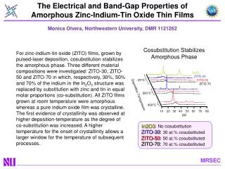
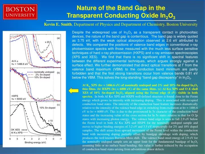
Nature of the Band Gap in the Transparent Conducting Oxide In2O3 Kevin E. Smith, Department of Physics and Department of Chemistry, Boston University Despite the widespread use of In2O3 as a transparent contact in photovoltaic devices, the nature of the band gap is contentious. The band gap is widely quoted as 3.75 eV, with the weak optical absorption observed at 2.6 eV attributed to defects. We compared the positions of valence band edges in conventional x-ray photoemission spectra with those measured with the much less surface sensitive techniques of hard x-ray photoemission (HXPS) and x-ray emission spectroscopies (XPS and XES). We find that there is no significant shift in spectral features between the different experimental techniques, which argues strongly against a surface effect. We further demonstrated that direct optical transitions at Γ from the valence band maximum (VBM) to the conduction band minimum are parity forbidden and that the first strong transitions occur from valence bands 0.81 eV below the VBM. This solves the long-standing ‘‘band gap discrepancy’’ in In2O3. Al K XPS (h = 1486.6 eV) of nominally undoped and 2% and 10%-Sn doped In2O3 thin films. (b) HXPS (h = 6000 eV) of the same films. (c) Al K XPS and O K shell XES of 10% Sn-doped In2O3 aligned using the Fermi edge (0 eV) visible in both spectra. In both Al K XPS and HXPS well-defined structure is found close to the Fermi energy which grows in intensity with increasing doping. This is associated with occupied conduction band states. The intensity of the conduction band feature increases dramatically relative to the intensity of the valence band edge in switching from excitation at h = 1486.6 eV to h = 6000 eV. This is due to the pronounced In 5s character of the conduction band states and the increasing value of the cross section for In 5s states relative to that for O 2p states with increasing photon energy. The valence band edge is seen to fall 2.9 eV below the Fermi level in both Al K XPS and HXPS for the nominally undoped sample and moves to higher binding energies of 3.2 eV and 3.5 eV respectively for 2% and 10% doped samples. The shift arises from upward movement of the Fermi level within the conduction band with increasing doping partially offset by bandgap shrinkage with doping, which produces the well known Burstein-Moss shift. The valence band onset energy of 2.9 eV for the nominally undoped sample sets an upper limit for the fundamental bandgap of In2O3 assuming little or no surface band bending: this value is further reduced by the occupation of conduction band states arising from adventitious donor defects