Download
1 / 14
140 likes | 377 Views
This presentation will probably involve audience discussion, which will create action items. Use PowerPoint to keep track of these action items during your presentation In Slide Show, click on the right mouse button Select “Meeting Minder” Select the “Action Items” tab

E N D
This presentation will probably involve audience discussion, which will create action items. Use PowerPoint to keep track of these action items during your presentation • In Slide Show, click on the right mouse button • Select “Meeting Minder” • Select the “Action Items” tab • Type in action items as they come up • Click OK to dismiss this box • This will automatically create an Action Item slide at the end of your presentation with your points entered. Nanolithography CHE 5480 Summer 2005 Maricel Marquez
Scanning Probe Lithography(SPL) • The Semiconductor Industry Association's 1997 National Technology Roadmap for Semiconductors predicts that critical dimensions will shrink to 150 nm by 2001, to 100 nm in 2006, and to 50 nm by 2012. • The conventional photolithography used for printing integrated circuit features is approaching fundamental limitations. An alternative lithography technology may be required within the next five years. • Scanning probe lithography (SPL) could be a viable alternative for patterning 100 nm feature sizes and • below.
4 Factors in SPL (1) Resolution, (2) Alignment accuracy, (3) Reliability, and (4) Throughput (wafers/hour).
HighResolution (SPL) • Scanning tunneling microscope (STM) or the atomic force microscope (AFM) is used to pattern nanometer-scale features. • When a voltage bias is applied between a sharp probe tip and a sample, an intense electric field is generated in the vicinity of the tip. This concentrated field is the enabling two effects: • Field enhanced oxidation (of silicon or metals) and electron exposure of resist materials.
Force Feedback. One loop maintains a constant small force (typically 10 nN) between the tip and the electron-sensitive resist.Current Control. The other feedback loop maintains a constant field emission current through the resist during exposure (generally in the range of 20 pA to 1 nA).
Cross-sectional SEM images of etched silicon features patterned by scanning probe lithography. (a) 50-nm-wide line written in SAL601 and etched 300 nm into the silicon using an HBr+O2 high density plasma (6:1 aspect ratio). (b) 26-nm-wide line written in PMMA and transferred through lift-off and anisotropic etching (NF3) into the silicon substrate. The etch depth is 260 nm, giving the line an aspect ratio of 10:1.
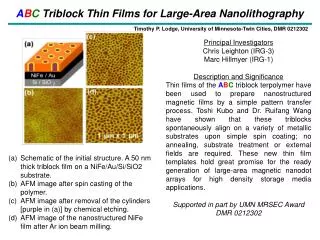
High Speed Patterning of Siloxene Spin-on-Glass • In order to pattern large areas in reasonable times, it is imperative to increase SPL writing speeds. For that purpose a resist material suitable for high speed writing has been identified. • The material is siloxene, a Si-O polymer with attached methyl groups, commonly known as Spin-on-Glass (SOG). • SOG can be easily patterned with electrons emanating from a scanning tip. High Speeds Patterns of 100 nm in SOG written using the AFM scanning at 1 mm/s. Other patterns have been written at 3 mm/s. Note: Dr. Quate’s website: http://www.stanford.edu/group/quate_group/LithoFrame.html