Download

1 / 19
190 likes | 360 Views
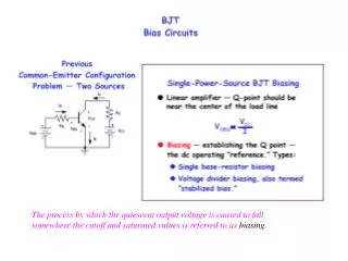
The process by which the quiescent output voltage is caused to fall somewhere the cutoff and saturated values is referred to as biasing. Example 3.13. Q-point has shifted Substantially. Q-point is not stabilized Against the variation . Tolerances - Worst-Case Analysis: Example.

E N D
The process by which the quiescent output voltage is caused to fall somewhere the cutoff and saturated values is referred to as biasing.
Q-point has shifted Substantially. Q-point is not stabilized Against the variation .
Tolerances - Worst-Case Analysis: Example • Problem: Find worst-case values of IC and VCE. • Given data: bFO = 75 with 50% tolerance, VA = 50 V, 5 % tolerance on VCC , 10% tolerance for each resistor. • Analysis: To maximize IC , VEQ should be maximized, RE should be minimized and opposite for minimizing IC. Extremes of RE are: 14.4 kW and 17.6 kW. To maximize VEQ, VCC and R1 should be maximized, R2 should be minimized and opposite for minimizing VEQ.
Tolerances - Worst-Case Analysis: Example (cont.) Extremes of VEQ are: 4.78 V and 3.31 V. Using these values, extremes for IC are: 283 mA and 148 mA. To maximize VCE , IC and RC should be minimized, and opposite for minimizing VEQ. Extremes of VCE are: 7.06 V (forward-active region) and 0.471 V (saturated, hence calculated values for VCE and IC actually not correct).
BJT SPICE Model • Besides capacitances associated with the physical structure, additional components are: diode current iS and substrate capacitance CJS related to the large area pn junction that isolates the collector from the substrate and one transistor from the next. • RB is resistance between external base contact and intrinsic base region. • Collector current must pass through RC on its way to active region of collector-base junction. • RE models any extrinsic emitter resistance in device.
BJT SPICE Model Typical Values Saturation Current IS = 3x10-17 A Forward current gain BF = 100 Reverse current gain BR = 0.5 Forward Early voltage VAF = 75 V Base resistance RB = 250 W Collector Resistance RC = 50 W Emitter Resistance RE = 1 W Forward transit time TT = 0.15 ns Reverse transit time TR = 15 ns Chap 5 - 19