Download
1 / 15
150 likes | 294 Views
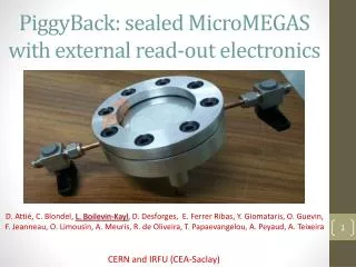
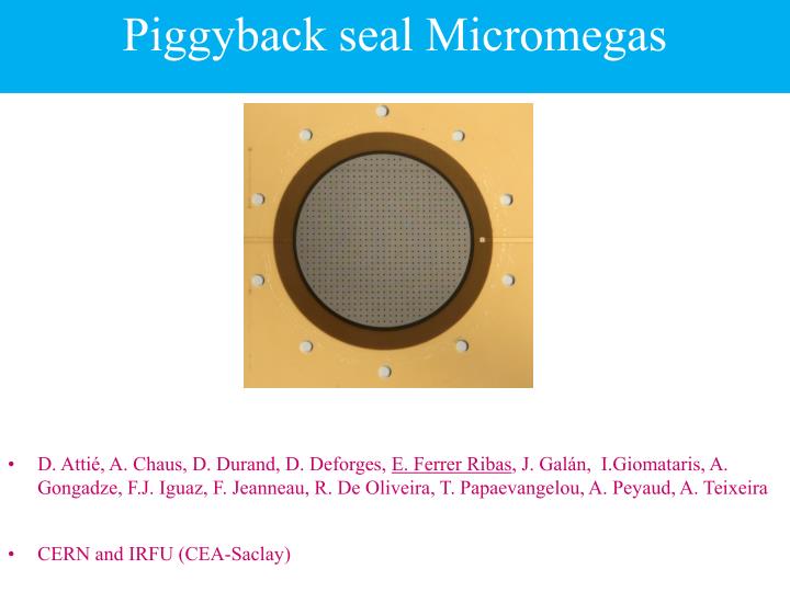
Piggyback seal Micromegas. D. Attié, A. Chaus, D. Durand, D. Deforges, E. Ferrer Ribas , J. Galán, I.Giomataris, A. Gongadze, F.J. Iguaz, F. Jeanneau, R. De Oliveira, T. Papaevangelou, A. Peyaud, A. Teixeira CERN and IRFU (CEA-Saclay). Concept.

E N D
Piggyback seal Micromegas • D. Attié, A. Chaus, D. Durand, D. Deforges, E. Ferrer Ribas, J. Galán, I.Giomataris, A. Gongadze, F.J. Iguaz, F. Jeanneau, R. De Oliveira, T. Papaevangelou, A. Peyaud, A. Teixeira • CERN and IRFU (CEA-Saclay)
Concept • Separation of the amplification structure and the readout plane Resistive layer (RuO2)~10 µm Resistive thin layer (1 MΩ /□ to 100 GΩ /□) Standard bulk structure • Signal is transmitted by capacitive coupling to the readout plane • Optimisation of the induced signal : tinsulator << tgasεinsulator/εgas • εinsulator should be as high as possible (first prototype alumina with ε~10 ) Insulator (Ceramic substrate~100-500 µm) Readout plane
First set-up -HVdrift -HVamp -HVresist Ground 3 detectors with active area: 3×3 cm2 1 cm drift, 128 µm amplification gap, 20 µm of RuO2 with 100 MΩ/□, ceramic layer 300 µm Argon + 5%Iso and Ne + 5% Ethane and a standard buk in Argon + 5%Iso I. Giomataris
First experimentalresults Checking possibles looses by the ceramic layer: signal entirely transmitted Test with a 252Cf (fission fragments signals) reading simultaneously mesh and anode Amplitude within 5% Same rise time for both polarities
Rate capability With X-rays from a gun (8keV) I. Giomataris
Comparison with Monte Carlo I. Giomataris
10 M/sq 100 M/sq 1 G/sq 10 G/sq I. Giomataris
CMOS chip readout Medipix2/Timepix CMOS chip 256×256 square pixels of 55 µm side each To be used with MPGD the MPGD needs to be covered by a layer of high resistivity material (amorphous silicon or silicon-rich nitride) Set-up with Piggyback 30×20 mm2 bulk Amplification gap 128 µm Drift gap 10 mm Signal observed on Medipix chip with Ar + 5% Iso No damage of the chip during operation at high gain 105
55Fe events (G ~ 50 000) Spot diameter about 500 mm With a ceramic plate of 100 mm We expect to get it down to 150 mm
Second set-up: towards a sealed detector Ar+5% Iso Gain
Second set-up: towards a sealed detector Detector chamber glued One night oven at 60°C + pumping Flushed with gas for only 4 hours Stability over 14 days
Latestresult for a sealed detector Piggyback resistive Micromegas , D. Attié et ale-Print: arXiv:1310.1242 [physics.ins-det] Stability over 30 days Small fluctuations due to day night effects Big amplitude fluctuation due to the removal of the source
Conclusions and outlook • Floating mesh, Bulk Micromegas, Microbulk, Ingrid and now Piggyback • Piggyback resistive Micromegas provides spark protection • Detector dissociated from readout plane • Can optimise dead space • High rate vs resistivity has been studied • Test higher values of resistivity, different thickness of ceramic • Seal detector is under development