Download
1 / 30
300 likes | 419 Views
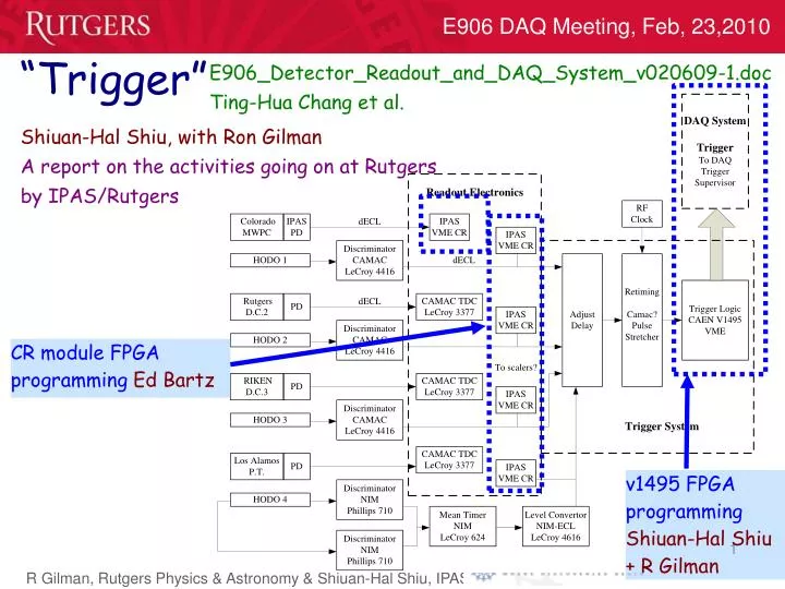
“Trigger”. E906_Detector_Readout_and_DAQ_System_v020609-1.doc Ting-Hua Chang et al. Shiuan-Hal Shiu, with Ron Gilman A report on the activities going on at Rutgers by IPAS/Rutgers. CR module FPGA programming Ed Bartz. v1495 FPGA programming Shiuan-Hal Shiu + R Gilman.

E N D
“Trigger” E906_Detector_Readout_and_DAQ_System_v020609-1.doc Ting-Hua Chang et al. Shiuan-Hal Shiu, with Ron Gilman A report on the activities going on at Rutgers by IPAS/Rutgers CR module FPGA programming Ed Bartz v1495 FPGA programming Shiuan-Hal Shiu + R Gilman
Trigger Interface Module • CODA interacts with ROCs/SBCs in each VME crate through a ``trigger interface module'' that connects the ROCs with the trigger supervisor • Rutgers has committed to build these • Two basic types: ~$400 6-GeV type, available now, and $? 12-GeV type, not available for several months • Have obtained from JLab circuit board manufacturing information, but still need (very soon!) component information, and information on components not needed for multi-ROC system • Assembly time ~1 day per module 2
CR Module Status • Ed Bartz has developed FPGA – TDC code and VME readout code – using ~70% of FPGA gates. (We have used ~1/3rd of Ed's time for 3 months, rest has gone to LHC) • Basic coding is now done, and we have started initial testing / debugging of a programmed CR module 3
VME 250 MHz / 4 Phases Time Counter Time Window Register Event Number Base Addr Bank Switch Data In 1 TDC 1 External Memory (Used as Fifo) 16ns Access Time Data In 2 (Stop – Data) < Time Window Event Builder TDC 2 Dual Buffer 32 bit x 32 Words MUX Data In 3 TDC 3 Data In 4 2 bit Cntr TDC 4 Data Word Count Error Flags 250 MHz (x16) Stop Count Stop TDC Block Diagram (24bit) Resolution is 1ns Need at least 128 ns between two events This utilizes all available Internal memory on the FPGA Limit: 1 Pulse/Chan every 16ns But need 8.3 µs before the buffer is all processed and the 3rd event hits appear Deadtime: (will send out a busy signal) 128ns to switch buffers between events. 8.3ɥs to build event (i.e. empty buffer, subtract stop time, load Fifo).
Couple notes • FIFO memory read/write access takes 16 ns, but VME read requests will occur ~1 us apart • To limit dead time, Ed has handshaking code so writing to FIFO memory is briefly interrupted by VME readout request • 128 ns dead time between events is not considered an issue – need ~ 1 us anyway for chamber drift time • 8.3 us for 3rd event is ~1% issue? Can try to increase # of buffers from 2 → 4, or simple reduction of buffer size to 4 words 5
- P P P P Data: P - - - - - - - - 0 - 24 Bit Data (Stop time – Time of Rising Edge) Channel # . Channel # Data: P 0 24 Bit Data (Stop time – Time of Rising Edge) - All Data is 32 Bit - - - - - 0 0 - - - - - - - - - - 1 0 0 1 TDC Data Format (All Times are in nanoseconds) - - - - Start: 24 Bit Event Number 1 1 1 . . Stop Cnt 1: 1 16 LSBs of Stop Count Time - - - - - 1 16 MSBs of Stop Count Time Stop Cnt 2: 12 Bit board address - - - - End: 1 - - 6BitErrFlags 10 Bit Event Word Count Error Flags: Bit 0: 32 Bit Time Counter Overflow Bit 1: Subtraction error overflow during Data Compaction Bits 2-5: Unused
TDC Memory Map Base Address: 0xABC000 A: Hex Switch A23-A20 B: Hex Switch A19-A16 C: Hex Switch A15-A12 Base Address: Write - Bits 23 - 0 – Time Window Register. Bit 24 = Reset TDC. Bit 25 = Reset Time Counter (to be added) Read - Bits 23 - 0 – Time Window Register. Bits 29 - 24 – Number of Events in Fifo. Base + 0x4 : Returns Base Address Switches. Base + 0x8 & 0xC : Returns Test Data (0x76543210 & 0xFEDCBA98). Base + 0x800 to 0xFFF : Returns Next Data from External Memory Fifo.
TDC Status & Future Plans Status: Design: All Features Detailed above are implemented. Testing: In Progress. Future Plans: Add Reset to Time Counter from VME and External Signal. If space allows, Add Pulse Counter to each data Input.
V 1495 Resources 4 CAEN v1495s on hand (2 IPAS, 2 RU) Sufficient additional A395A input boards on hand (6 IPAS, 2 RU) Two A395C ECL output board on hand (2 RU) All needed special cables on hand (all RU) 1 VME crate from FNAL, 1 TS/VME crate from JLab 2 SBC/ROCs/MVME6100s (RU) Currently have for testing: FNAL: 2 pulsers, 4 level shifters (Phillips + LeCroy), RU: 3 function generators, 1 level shifter, 1 scope 1 graduate student to do the real work (Shiu Shiuan-Hal)
V 1495 Programming V1495 provides a user-programmable Altera Cyclone EP1C20 FPGA – 20,060 4-input logic elements, 295 kbits RAM, up to ~400 MHz operation (for some functions) CAEN provides “quartus II” for programming v1495, along with a number of simple programming examples – eg, 16x16 PLU Procedure: Edit vhdl with quartus on windows machine Compile Transfer to DAQ machine (email, memory stick...) ROC can read DAQ machine hard drive to access v1495 code Flash to v1495
V1495 Simple / Sample Trigger Matrix / Track Program - 1D “Toy” Example: 3 hits / 4 planes, inputs on A, B, D, E, output on C: if( (A( 1)='1' AND B( 1)='1' AND D( 1)='1' ) OR (A( 1)='1' AND B( 1)='1' AND D( 2)='1' ) . . . OR (B(32)='1' AND D(32)='1' AND E(32)='1' ) ) then C(3)<='1'; elseif C(3)<='0'; end if; Tested with up to several thousand conditions coded, several input conditions all led to output in < 40 ns
The role played by V1495 Hodoscope Discriminator level shifters ɥ- Yeeeeeeeehaaaaaa!! x4 Second level V1495 First level V1495
V1495 System Architecture Original plan: 3 v1495s: 2 to do tracks in X/Y → lower/upper halves of detector, with 2 32-bit outputs to v1495 track correlater (given 160 input channels) Concern: trade offs between speed of trigger, resolution of information passed to second level, problems with multiple tracks, …
Some possible V1495 System Architecture ?1: 5 v1495s: 4 to do tracks in 4 quadrants, with 32-bit outputs to v1495 track correlater – twice as much information transferred, efficiency problems at edges. ?2: 5 v1495s: 4 in lower X, lower Y, upper X, upper Y, with 32-bit outputs, but transfer all paddle hits in 3 times multiple clock cycle to v1495 track correlater. All data processing done in the second level v1495 – are the 20,000 logic elements enough for all desired triggers? ?3: 3 v1495s: 1 tracks all X, 1 tracks all Y. With 32-bit outputs and transfer data in multiple clock cycle to v1495 track correlater to triple information – even efficiency, but issues from resolution and multiple tracks Monte Carlo simulation needed to help choose best scheme.
Track correlater Original plan: Since “front” FPGAs look at entire halves of detectors, expect to be able to eliminate vertical inefficiency band Possible plan: The S1 scheme has the vertical andhorizontal inefficiency band. The S2 and S3 scheme can also eliminate the horizontal and vertical inefficiency band. How important is this? Is track rate so high in horizontal plane that we want an inefficiency stripe there? Intuitions please! C.A. Gagliardi et al., "Hardware Trigger System for Fermilab E866", Nucl. Instrum. Methods A 418, 322 (1998)
Flow chart of transfer data in multi clock cycle 160 bits data All X/Y plane Look Up Table Data collect Look Up Table Trigger 32 bits . . . 32 bits Second level FPGA Front level FPGA 3ns 6ns 6ns 39ns 39~49ns 93~103ns
Advanced information transfer We using 3 bits to let the second level v1495 identify the signal as the first, second, or third part of the data transfer. For example: First part Second part Third part Because of the limit working frequency of the input/output port (200MHz), and 53 MHz beam, we can only “overclock” data transfer by a factor of 3 (32 bits → 87 bits). At present overclocked data transfer does not have any mechanism to avoid transfer failures. (Example: first level does not sent correct sequence to second level.) Need to think about how to deal with this.
Future work!! Keep testing the TDC. Continue to work on stability of overclocking the data transfer between v1495s. Try to build up some mechanism to avoid transfer failures. Looking into Mc for generating trigger matrix up to date geometry database needed.
Desired Triggers Two opposite charged tracks, hits on all four planes, in opposite quadrants pointing towards target Two tracks: Some planes missing hits Same charge Not opposite quadrants Do not point at target Multiple deficiencies? Single track pointing at target Single track, but planes missing hits, does not point at target? Multiplicity trigger: n planes hit Random in time or pulser trigger Cosmic trigger?
Trigger Discussion Assume: 8 hodoscopes, each 2 rows of 16 paddles, so 256 signals Need to prioritize triggers, for limited number of CODA trigger types Need to worry about timing to produce the various trigger types that come from one set of input data Do we want to insist on hits on every plane for a track? What is sufficient for efficiency triggers? (Single vs double tracks?) For tracking: can we divide the hodoscopes up into 4 quadrants that we analyze independently – do we have to be concerned about edge effects? With multiplicity trigger, do we need cosmic trigger?
Trigger Supervisor TS and crate borrowed from Jlab (TS from David Abbott) Put triggers into TS and tested that we could read out internal registers that count number of triggers successfully Did not implement into DAQ system Recall that TS is not needed for a single-crate DAQ system, but is needed for multi-crate systems. Will need additional cables for enabled/busy hand-shaking with readout electronics
DAQ System Set up CODA 2.6 DAQ system with MVME6100 ROC, generating pseudo-data in ROC – no actual readout modules Similar to IPAS setup previously described by Wen-Chen Chang Partially documented in password protected “elog” at https://906daq.rutgers.edu:8080/906daq/ More stream of conscience than wiki-like
Coincidence Register Modules FPGA based TDCs, and maybe scalers IPAS needs additional resources for programming Ed Bartz, Rutgers P&A electronics, expects to begin work in next ~week on these, after we get him spec / documentation / modules Previous experience with several FPGA projects, for CMS etc. Wants in particular to understand priorities / trade offs, in case these are needed Had 2 ~hour-long discussions, sent Ed talks from January and April '09 Expects ~2 month project for TDC, unsure if there would be much time savings for programming as a scaler Is Ed handling TDC or TDC + readout?
CR Questions What is output? Number of data words in event, channel and time of each hit within some time interval before level 2 trigger Is time absolute or relative to L2 trigger? We also output L2 trigger time with some special channel number? Is clock 64 bit? 64 bit clock * 1 ns ~ 2x10¹⁰ s ~ 600 years CODA likely reads out 1 event at a time, although buffer lowers dead time. Also requires event number counter in module that can be reinitialized at start of each run?
Information passed to track correlater Straightforward, fast scheme that can handle multiple tracks: From each of 2 “front-end” Y v1495s: set bits to indicate position track passes in 1st scintillator hodoscope plane – 16 bits for each quadrant corresponds to number of paddles. Generally more than 1 bit set if there are multiple tracks. Can reduce resolution to leave special status bits – no plane 4? From each of 2 “front-end” X v1495s: set bits to indicate position track passes in 1st scintillator hodoscope plane – 8 bits for each quadrant position leaving 16 bits to set for momentum of track (8 bits + and 8 bits -) Note: for multiple tracks position+momentum correlation is lost in this scheme. Need experienced intuition / MC study to optimize scheme
Track correlater From patterns from “front” FPGAs, identify possible trigger types, and set output bits to send to trigger supervisor Philosophy: better to accidentally include some, eg, not opposite quadrant μ +μ - pairs than to be inefficient at finding them Have not tested conflicts in FPGA outputs where different logic conditions try to set contradictory output bit patterns CODA trigger supervisor handles multiple trigger types arriving at “same” time, but we have to be careful about counting one event as multiple trigger types for scaling / dead time corrections.
Advanced information transfer Shiuan-Hal is studying advanced schemes to improve triggering Data compression and transfer over multiple clock cycles allows more detailed information to be passed to the track correlator, thus a better trigger, but at the cost of more processing time. We are pretty confident the simple scheme allows a trigger in ~100 ns. How much time do we have / by when is the trigger needed?