Download
1 / 10
100 likes | 131 Views
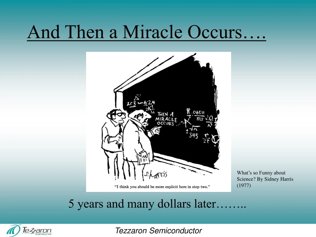
And Then a Miracle Occurs…. 5 years and many dollars later……. What’s so Funny about Science? By Sidney Harris (1977). A Closer Look at Wafer-Level Stacking. “ Super-Contact ”. Oxide Silicon. Dielectric(SiO2/SiN) Gate Poly STI (Shallow Trench Isolation). W (Tungsten contact & via)

E N D
And Then a Miracle Occurs…. 5 years and many dollars later…….. What’s so Funny about Science? By Sidney Harris (1977)
A Closer Look at Wafer-Level Stacking “Super-Contact” Oxide Silicon Dielectric(SiO2/SiN) Gate Poly STI (Shallow Trench Isolation) W (Tungsten contact & via) Al (M1 – M5) Cu (M6, Top Metal)
Stacking Process Sequential Picture Two wafer Align & Bond Course Grinded Fine Grinded After CMP Si Recessed
Grinding Striation at Center Grinding Striation at Middle Grinding Striation at Edge Grinding striation vanishes after CMP on pattern wafer Striation caused by grinding disappears after CMP, depth of striation not more than 0.10 µm
Stacking Alignment, Infra Red Microscope Images VERNIER_X-axis Misalignment Tezzaron’s Alignment Target Wafer Left (-80mm,0) Wafer Right (+80mm,0) Wafer Left (-80mm,0) Wafer Right (+80mm,0) VERNIER_Y-axis Misalignment Staked wafer picture Wafer Left (-80mm,0) Wafer Right (+80mm,0)
High Precision Alignment Misalign=0.3um Top wafer Bottom wafer
Then, Stack a Third Wafer: 3rd wafer 2nd wafer 1st wafer: controller
Finally, Flip, Thin & Pad Out: 1st wafer: controller 2nd wafer 3rd wafer This is the completed stack!