Download
1 / 11
110 likes | 211 Views
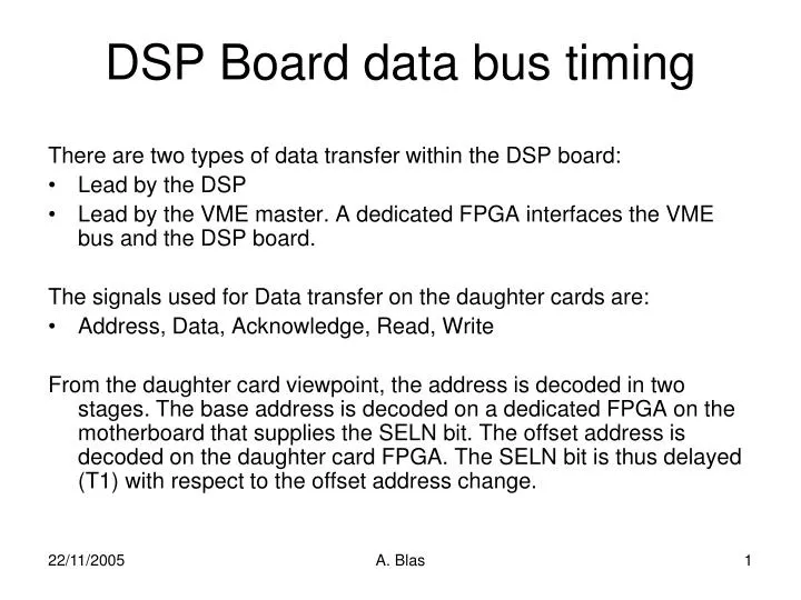
DSP Board data bus timing. There are two types of data transfer within the DSP board: Lead by the DSP Lead by the VME master. A dedicated FPGA interfaces the VME bus and the DSP board. The signals used for Data transfer on the daughter cards are: Address, Data, Acknowledge, Read, Write

E N D
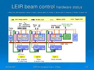
DSP Board data bus timing There are two types of data transfer within the DSP board: • Lead by the DSP • Lead by the VME master. A dedicated FPGA interfaces the VME bus and the DSP board. The signals used for Data transfer on the daughter cards are: • Address, Data, Acknowledge, Read, Write From the daughter card viewpoint, the address is decoded in two stages. The base address is decoded on a dedicated FPGA on the motherboard that supplies the SELN bit. The offset address is decoded on the daughter card FPGA. The SELN bit is thus delayed (T1) with respect to the offset address change. A. Blas
DSP Board data bus timing A. Blas
Address decoding PROBLEM: As the base address is delayed (T1) with respect to offset address, what tells us when the address is really valid? Making the product of the 2 decoders (base and offset) might give false information before and after the actual addressing (see p.2) Enabling the decoder output when both base and offset addresses are decoded for longer than T1 gives a valuable result at the beginning of the cycle, but can be fooled at the end. Using the read/write signals to gate the address decoding doesn’t help as they might be active when the decoding is fooled. Using the rising edge of read/write to reset the decoder at the end of the cycle could be ok if we knew how long to apply this reset. When the DSP is mastering the bus, only do we know that this time should be greater than 2.125ns+h*Tck, and when the VME is leading, either should it be negative! (VME reading) or not specified (DSP writing) (address pipelining mode should be taken into account; i.e.: the next address is sent before the end of the cycle. A. Blas
Address decoding Attempt solution: use the falling edge of either read or write to start a timer. After a time T2 >T1 memorize the address decoder output to use it as bus-access-enable. Use then the leading edge of read/write to reset the bus access register. This method requires to program the DSP wait register such as to have W*25ns > T2. To make the circuit compatible with the present VME interface circuit, one needs also to fulfill T2 < 3*Tclk (Tclk being the clock used in the VME interface circuit = 25 ns) Downside of this solution: with the present VME interface, the rising edge of RDH comes 2*Tpd (propagation time within the VME interface = 6 ns?) after the change of address when the VME is leading the bus. This might cause some conflicts on the bus. Conclusion: I didn’t find yet a really proof solution with this addressing in two delayed parts. In the next revision of the mother board, this topic should be tackled. This easiest, may be, being to have all the bus components following the same track (delayed in the same way). A. Blas
Address Decoding circuit A. Blas
Output register circuit A. Blas
Output I/Q register circuit A. Blas
DSP reading bus A. Blas
DSP writing onto bus A. Blas
VME reading Bus A. Blas
VME writing onto bus A. Blas