Download
1 / 27
270 likes | 355 Views
Fabrication of crystals for channeling at INFN. Vincenzo Guidi. Sensors and Semiconductors lab University of Ferrara and INFN - Italy. Fermilab, December 6-7, 2007. Outlook. Sample preparation Treatment of surfaces Surface characterization

E N D
Fabrication of crystals for channeling at INFN Vincenzo Guidi Sensors and Semiconductors lab University of Ferrara and INFN - Italy Fermilab, December 6-7, 2007
Outlook • Sample preparation • Treatment of surfaces • Surface characterization • Participation to H8RD22 experiment(CERN, IHEP, INFN, JINR, PNPI) • Interest in collimation experiment at FNAL
Dicing of crystals I Si samples for channeling are achieved from wafers or ingots. Proper sizing of the crystal to the wanted application involve dicing and other operations that partly damage the surface of the crystal
c Dicing of crystals I Si samples for channeling are achieved from wafers or ingots. Proper sizing of the crystal to the wanted application involve dicing and other operations that partly damage the surface of the crystal Mosaicity is being generated at surfacewhich is often of the order of the critical angle of impinging particles
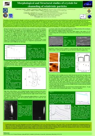
Dicing of crystals II Crystals were diced from a commercially available wafer using a fine-grit blade to minimize the mechanical damage during the cut. Diamond grain: size = 4-6 m Density = 62% Dicing speed: 0.5 mm / min Diamond blade Dicing machine
Isotropic chemical etching Planar etching erodes the surface of a crystal layer by layer. • HNO3 oxides Si to SiO2 • HF erodes SiO2 • CH3COOH as a solvent Planar etching erodes the surface of a Si crystal layer by layer HF, HNO3, CH3COOH (2:15:5)
RBS - channeling mode Rutherford backscattering under channeling mode is a powerful method to investigate the structure of a surface Channeled particles penetrate deeper into the crystal and are more difficult to emerge out of the surface, resulting in a decrease of the current
RBS spectra > 12m Chemical etching I APL 87(2005)094102
As-cut Chemical etching Mechanicalpolishing AFM analysis
Roughnessanalysis As cut We observed roughness increase with chemical etching CE1
Etching vs. polishing Measurements taken in an external beam line at IHEP with 70 GeV protons Mechanically polished surface Chemically etched surface RSI 73(2002)3170
beam Experiment H8RD22 1-mrad-accuracy goniometer • Multistrip detectors • (10/30 mm spatial resolution) • AGILE type • AMS type • External line H8 of the SPS • 400 GeV/c protons • < 8 mrad divergence Spokesman: Dr. Walter Scandale
θref λ Volume reflection Unchanneled particle Uo d Channeled particle Volume-reflected particle Volume-captured particle Volume reflection was predicted by Taratin and Vorobiov In 1988 Channeled particle
6 4 (b) 5 2 3 1 (a) Observation of VR • Primary beam • Channeling • Dechanneling • Volume reflection • Volume capture • Primary beam PRL 98(2007)154801 Measurements with sample ST4 (now here at FNAL) • Deflection occurred at about 13.5 mrad • Fraction of diverted particles larger that 97% • Large acceptance
Demand for lower roughness An application of crystals would be the collimation of beam halo in next generation of hadron machines (e.g. the LHC) Particles in the halo drift outwards at the rate of ~2 nm per turn. Since the tune is not integer, the particles will hit the crystal every ~10-20 turns and thereby the first impact parameter of the particles onto the crystal will be in the range of ~100 nm (curtesy of V. Previtali and R. Assmann) It demands a crystal with a roughness lower than 100 nm on the lateral faces of the crystal
Rivisiting chemical etching Formation of a morphologically non homogeneous surface may be prevented by an unusually large concentration of HNO3 Oxidation of Si by HNO3preferentially begins at the defects forming nitride oxide, which locally catalyzes further the oxidation reaction in the neighboring area and finally results in formation of a crater. An excess of HNO3 strengthens the oxidation, which involves the whole surface nearly at uniform rate. Properly short timing for reaction leads to defect removal leaving a smooth surface
AFM analysis As cut New CE Old CE Significant decrease in roughness was observed with the new CE
RBS spectra 4He+ Low signal of backscattered particles means good crystalline quality p Chemical etching II APL 91(2007)061908
Structure of the surface The surface min is defined as the ratio of the RBS yield under channelling alignment and random condition extrapolated at the surface channel. The higher the degree of crystalline order in the lattice the lower the surface min due to the reduction of dechanneling from the defects in the crystal. Experimental min for a Si [110] sample with probe particles of 2 MeV. An ideally perfect surface yields min = 2%
Anisotropic etching Anisotropic etching is a feasible way to realize highly flat damage free surfaces of crystals entirely by wet chemical methods Etch rate on different silicon planes for KOH 20% at 40 °C nanometric roughness was achieved
Photolythography a) Starting material: (110) silicon wafer b) LPCVD deposition of silicon nitride thin layer c) Silicon nitride patterning d) Etching of Si in KOH solution, silicon nitride acts as masking layer e) Silicon strips release f) Removal of silicon nitride
VR vs. bending radius Inefficiency vs. curvature radius Deflection angle vs. curvature radius
Multistrip crystal 2mm 2mm Frame Cross section Silicon strips Thickness: 0.5mm 70mm
Multiple VR with multistrip • We were able to align up to 4 strips • With 3 strips, deflection angle is 40.5 μrad • Reflection efficiency is 93%
Deformation of the frame Anticlastic bending in a strip Because of the frame, global deformation of the crystal occurs Ideal alignment condition
Ultra-thin frames • Realization of ultra-thin frames • Verification of independence of rotation of each strip
Interest in collimation project at FNAL • Provision of crystals (yes) • Characterization of crystals (yes) • Refurbishing of previously used crystals, e.g. O-shaped crystal (yes) • Participation in experimental runs (yes) • Detectors (to be determined) • Other issues (e.g. goniometer requested)