Download
1 / 25
250 likes | 369 Views
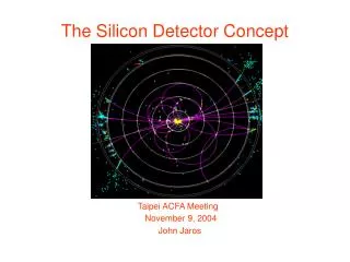
Sergo Jindariani Fermilab (on behalf of the CDF II Silicon group). Operational Experience and Longevity Studies in the CDF II Silicon Detector. 2010 Vienna Conference on Instrumentation Vienna, Austria, Feb. 15 - 21, 2010. CDF Run II Detector at Tevatron.

E N D
Sergo Jindariani Fermilab (on behalf of the CDF II Silicon group) Operational Experience and Longevity Studies in theCDF II Silicon Detector 2010 Vienna Conference on Instrumentation Vienna, Austria, Feb. 15 - 21, 2010
CDF Run II Detector at Tevatron Tevatron:proton-antiproton collider at √s = 1.96 TeV Run II: 2001–2011 (2012?) Luminosity: 7 fb–1delivered (Oct ’09) Two multi-purpose detectors: CDF & DØ • CDF II:Standard HEP detector with excellent tracking • silicon detectors • large open-cell drift chamber for a broad physics program S. Jindariani, VCI 2010
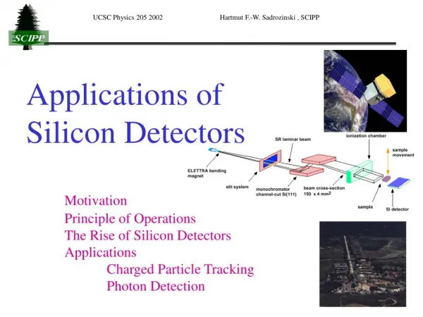
CDF II Silicon Detectors Overview: • Three components: SVX-II, ISL, L00 • 7-8 layers, 722k readout channels • 7 m2 of silicon strips • 3D hit information from DSSDs • Forward tracking with ISL and improved vertexing with L00 SVX: Double sided silicon Layers 0,1,3 with rφ/rZ (Hamamatsu) Layer 2+4 Micron ISL: additional layers, SaS Hamamatsu+Micron add forward coverage L00: LHC-style silicon, single-sided, actively cooled “Narrows” (SGS Thomson and 2 Micron [Oxygenated]) “Wides” (Hamamatsu) S. Jindariani, VCI 2010
Sub-detector: SVX II • SVX II: The core of the silicon systems • Overall dimensions: • 1 meter along beam direction • Radii from 2.5 to 10.6 cm • Structure: three identical barrels • 2 bulkheads • 12 wedges • 5 concentric silicon layers • Silicon layers • Strip pitch: 60 to 140 mm • Layers 0,1 and 3(Axial and 90º strips) • Layers 2 and 4(axial and 1.2º strips) SVX II before installation SVX II barrel S. Jindariani, VCI 2010
Sub-detector: L00 • Layer 00: Right onto the beam pipe • Overall dimensions: • 1 meter along beam direction • Radii from 1.2 to 2.1 cm • Structure: • 2 bulkheads • Three consecutive sensors • 6 wedges • Silicon layers • Strip pitch: 25 mm • Axial strips • Radiation tolerant (LHC style) L00 during installation 1.2 cm 2.1 cm S. Jindariani, VCI 2010
Sub-detector: ISL • ISL: Intermediate Silicon Layers • Overall dimensions: • 1.9 m along beam direction • Radii from 20.5 to 29 cm • Structure: three different barrels • Central: Single layer,14 wedges • Forward:Two layers,12 and 18 wedges • Each barrel two bulkheads • Silicon layers • Strip pitch: 55 mm • Axial and 1.2º strips ISL sensors S. Jindariani, VCI 2010
Silicon Operations Group Silicon Project Leaders Working Groups On-Call Experts Detector Silicon Main Pager Carrier DAQ Power Supplies Cooling/Interlock Pager Carrier Cooling/Interlock Monitoring Backup Pagers DAQ/Detector Studies Power Supplies S. Jindariani, VCI 2010
Maintenance is a Challenge This is as close as we can get • Timeline: • R&D – 4 years • Production and Installation – 1 year • Commissioning - 1.5 years • Complex system: • 722,000 channels • 5400 chips • Cooling and Interlocks • Lots of cables • Various problems • Power Supplies • ISL Cooling • Wirebond Resonance problems • Beam Incidents • Infrastructure and Aging S. Jindariani, VCI 2010
Operational Issues During commissioning: • Blocked Cooling lines • Blocked by glue, well inside the detector • Solution: open them up with a powerful laser • Resonances • Wire bonds to the magnetic field • Synch. Readout wire oscillate and break • Solution: Stop high frequency synchronous readouts. • Beam Incidents • High dose accidentally delivered to the detector • Solution: • Collimators in key parts of the Tevatron • New Diamond based BLM system. After commissioning: Infrastructure & Aging B Jumper groove left by beam S. Jindariani, VCI 2010
Power Supplies • Common failure modes of CAEN SY527 • Communication loss • Corrupted read back of voltages/currents • Spontaneous switch off • Failure mode of power supply modules: • Voltages in Analog, Digital and Port-Card supply start slowly dropping. • Most Power supplies started to show this. • Problem: • aging of one type of capacitor • 36 capacitors per power supply • Can result in bit errors • Solution: • Work during shutdowns in 2007 and 2009… • take all faulty power supplies out • replace all 36 capacitors (on FNAL site) • put them back in and test them on location. • Time intensive effort, lasted about 2 months. • Not enough time to change all at once • Some need to be shipped to CAEN • Still expect to replace others as failure appears All power supplies with this failure were replaced! S. Jindariani, VCI 2010
ISL cooling repairs • Work during shutdowns of 2007 and 2009: • Keep the silicon cold and dry at all times • A plastic tent was setup to work. • A custom made air dryer changed the volume every 2 minutes. • Dew Point was always kept below -10 Cº. • Basic Idea: • Cover holes with epoxy from the inside of the pipe • using borescopes and catheters. • Repairs took a month • 4 shifts of people • Current status: • Tight vacuum in the repaired lines • Repairs of conical manifolds are needed Hole Repaired cooling system has been running stable! S. Jindariani, VCI 2010
Actions Taken to Maximize Longevity • Following the 2004 recommendation of the CDF Run II silicon task force the following measures were taken to maximize detector longevity: • Run colder: SVXII+L00 and ISL operating temperatures were lowered from -6, 10 oC to -10, 6 oC. • Identify/fix DAQ channel failure modes: • Installed electronics to prevent wire-bond resonances • Installed protective shield (baggy) to minimize thermal cycles of the detector during an access, which prevents e.g. DAQ chip front-end (AVDD2) failures • Safeguard against Tevatron beam incidents: • positioned beam collimators optimally • installed extensive beam monitoring tools to power off the sensors under abnormal beam conditions • asked the Tevatron operations to minimized abort kicker pre-fires which caused a significant fraction of DAQ chip damage • Regularly monitor change in depletion voltage: This helps in identifying a problem at its onset and e.g. go colder if necessary S. Jindariani, VCI 2010
Performance • Inner layers are in severe radiation environment. • Detectors were designed for Run IIa (2-3 fb-1) and now expected to acquire ~10 fb-1. • Currently ~90% ladders integrated, ~80%good (< 1% error rate), ~10% bad with an average error rate of 10% • Great performance after 8 years of running! • In addition, aging electronics, cooling system, depleting spare pool etc. A “ladder” is the smallest detector building block comprised of 2-4 sensors, 4-16 readout chips and read out via a High Density Interconnect (HDI) S. Jindariani, VCI 2010
Radiation Field Measured using more than 1000 thermo-luminescent dosimeters (TLDs) Two different data-taking periods allowed for distinction between fields: Radiation field is collision-dominated and scales with due to beam losses due to pp collisions p p (See R. J. Tesarek et al., IEEE NSS 2003) How this field affects the silicon sensors ? S. Jindariani, VCI 2010
Radiation Damage (Aging) Two general types of radiation damage to the sensors: • Bulk (Crystal) damage due to Non- Ionizing Energy Loss (NIEL) leading to displacement damage, build up of crystal defects. • increase of shot noise, change of effective doping concentration, increase of charge carrier trapping, etc. • Surface damagedue to Ionizing Energy Loss (IEL) causing accumulation of charge in the SiO2 and the Si/SiO2 interface. • Inter-strip capacitance (noise factor), breakdown behavior etc. The inner layer SVX-L0: ⇒ Inability to deplete the sensors: breakdown of AC-coupling capacitors @ ∼150 V ⇒ Increased noise from the sensors: degraded signal to noise ratio (S/N) Bulk damage to the sensors is the main concern for detector longevity S. Jindariani, VCI 2010
Aging Studies – Variables of Interest • Information on integrated radiation dose in a sensor is obtained by • evolution of bias current: provides “direct” information on the bulk condition, due to increase in leakage current. Change in leakage current is linear with the absorbed dose, ∆Ileak = α ∆Φeq , measured in 1-MeV neutron equivalent fluence [cm−2], where α is the damage factor. It is dependent on sensor temperature. • evolution of depletion voltage: gives information on our ability to deplete the sensors in the future. Its extrapolation predicts the need to raise applied bias voltage and its limit. • Performance of the aged detector is obtained by • Signal-over-noise (S/N) studies: provide estimates of usability of the detector in charged particle tracking and in turn for physics analyses. S. Jindariani, VCI 2010
Depletion Voltage: Signal Vs Bias • Look at the charge collection distribution • Reconstruct a track w/o using the studied sensor • If track points to hit in sensor record its charge • Charge collection distribution • Follows a landau distribution • Distribution is smeared by intrinsic noise • Fit the curve to a Landau convoluted by Gaussian(4 parameter fit) • Depletion Voltage: • Maximal for a fully depleted sensor • Study charge collection as function of VBIAS • Identify charge of Most Probably Value (MPV)in each distribution S. Jindariani, VCI 2010
Depletion Voltage Study -- Signal Vs. Bias • Plot charge’s Most Probable Value (MPV) for different bias voltages • Fit to a sigmoid (parameters include the plateau of maximum charge) • Define depletion voltage, Vd , as voltage that collects 95% of the charge at the plateau • Depletion Voltage as a function of integrated luminosity • 3rd order polynomial fit around the inversion point • Linear fit to extrapolate to the future S. Jindariani, VCI 2010
Depletion Voltage Projection • Prediction for L00 • Depends on type of sensor • Oxygenated ladders invert much later • Prediction for SVX-L0 • Bulk of ladders will survive • First symptom: micro-discharges We will be able to fully deplete most of the sensors beyond 10 fb-1 S. Jindariani, VCI 2010
Study of Signal to Noise Ratio • The figure of merit of the sensors’ physics performance is the Signal to Noise Ratio (S/N) • Signal: charge collected when a charged particle crosses the sensor • Noise: intrinsic noise of the detector • Signal • Use J/y m+m- tracks • Get total charge of cluster • Decrease linearly with Lumi. • Mean Strip Noise • Average over strips in charge cluster • Obtained from calibrations taken every two week. • Square root increase with Lumi. S. Jindariani, VCI 2010
SVXII Signal / Noise Projection r-phi z Tracking performance of SVX-L0 will be adequate beyond 10 fb-1 S. Jindariani, VCI 2010
Summary and Conclusions Operations - Expect the unexpected • Infrastructure is important • Expertise is important • Timely addressed all operational problems • Very Stable Performance Aging: • The inner layers have long progressed through inversion and exhibit consistent post-inversion behavior. • Most ladders in SVX-L0 and SVX-L1 layers would be operable up to 10 fb-1. The innermost layer, L00, is expected to compensate for any lost tracking and vertexing performance. The CDF Run II Silicon Detector will continue successful operation for the rest of Run II !! S. Jindariani, VCI 2010
BACKUP SLIDES S. Jindariani, VCI 2010
Actions Taken to Maximize Longevity • Following the 2004 recommendation of the CDF Run II silicon task force the following measures were taken to maximize detector longevity: • Run colder: SVXII+L00 and ISL operating temperatures were lowered from -6, 10 oC to -10, 6 oC. • Identify/fix DAQ channel failure modes: • Installed electronics to prevent wire-bond resonances • Installed protective shield (baggy) to minimize thermal cycles of the detector during an access, which prevents e.g. DAQ chip front-end (AVDD2) failures • Safeguard against Tevatron beam incidents: • positioned beam collimators optimally • installed extensive beam monitoring tools to power off the sensors under abnormal beam conditions • asked the Tevatron operations to minimized abort kicker pre-fires which caused a significant fraction of DAQ chip damage • Regularly monitor change in depletion voltage: This helps in identifying a problem at its onset and e.g. go colder if necessary S. Jindariani, VCI 2010
SEUs in CDF Collision Hall Electronics • CAEN PS crate auto-reset rates in their collision hall locations. Slight rise over time. FIB crate SEUs on the rise Mitigation studies ongoing. N-E corner is worst hit S. Jindariani, VCI 2010