Download
1 / 62
620 likes | 715 Views
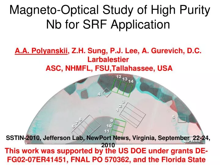
Magneto-Optical Study of High Purity Nb for SRF Application A.A. Polyanskii , Z.H. Sung, P.J. Lee, A. Gurevich, D.C. Larbalestier ASC, NHMFL, FSU,Tallahassee, USA SSTIN-2010, Jefferson Lab, NewPort News, Virginia, September 22-24, 2010.

E N D
Magneto-Optical Study of High Purity Nb for SRF ApplicationA.A. Polyanskii, Z.H. Sung, P.J. Lee, A. Gurevich, D.C. Larbalestier ASC, NHMFL, FSU,Tallahassee, USA SSTIN-2010, Jefferson Lab, NewPort News, Virginia, September 22-24, 2010 This work was supported by the US DOE under grants DE-FG02-07ER41451, FNAL PO 570362, and the Florida State
MOTIVATION • The recent studies showed that superconducting cavity performance is very sensitive to quality of Nb surface. • The penetration of small numbers of flux lines into the cavity surface during RF operation is leading to breakdown of the superconducting state and causing Q-drop or quench. • Q-drop can be triggered by early flux penetration in hotsports leading to thermal breakdown on the cavity surface (1 and 2). (Model by A. Gurevich). • Local study of flux penetration is important
MOTIVATION Magnetization and Magneto-Optical Imaging (MOI) techniques can detect local magnetic flux penetrate in Nb
EXPERIMENTALTECHNIQUE : 1. MAGNETO-OPTICAL 2. VSM 3. SEM 4. ZYGO LIGHT MICROSCOPY by Z. H. Sung (See:www.zygo.com/?/products/nv6000)
Polarized light F=V Bz 2d GGG Ba,z d YIG: Bi Ba,x M PRINCIPILE OF MAGNETO-OPTICAL TECHNIQUE MAGNETO-OPTICAL INDICATOR ON BASE OF GARNET FILM DOPED BY Bi DETECTS MAGNETIC FIELD Protective layer Nb Reflective layer
THE FARADAY ROTATION IN A FERRIMAGNETIC Bi-DOPED IRON GARNET INDICATOR FILMS WITH IN-PLANE MAGNETIZATION LIGHT POLARIZATION
MAGNETO-OPTICAL CONTRAST PICKS UP ON PLASTIC REFRIGIRATE CARD: DISTRIBUTION OF STRAY FIELD AROUND MAGNETIC STRIPS
MO IMAGES OF MAGNETIC FIELD IN AUDIO TAPE AND COMPUTER DISCETS 500m 100m 3.5 inch disc Audio tape 5.25 inch disc
MO IMAGES OF MAGNETIC CODES IN DIFFERENT PLASTIC CARDS 500m (AAA) American Automobile Association Card Visa Credit Card Library Vendor Card
MAGNETO-OPTICAL IMAGING SETUP FOR SUPERCONDUCTING RESEARCH: electromagnetic system creates magnetic field in two direction: X and Z cryostat Polarized Optical Microscope Z Hext Hext X LHe
MAGNETO-OPTICAL SETUP ON THE BASE OF A POLARIZING MICROSCOPE IN REFLECTIVE MODE
GEOMETRY OF MAGNETO-OPTICAL EXPERIMENT ON Nb SAMPLES FOR CAVITY APPLICATION IN PERPENDICULAR-Z AND PARALLEL-X (IN-PLANE) FIELDS MO indicator with in-plane magnetizationdetects the normal component of magnetic flux Z MO indicator Demagnetization factor Nz>0 Nb Nb Nb Hext X Hz=(1/1-Nz) x Hext
MAGNETIC FLUX DISTRIBUTION IN RECTANGULAR SAMPLE: EFFECT OF SAMPLE SHAPE WITH DEMAGNETIZATION FACTOR Nz>0. (“roof pattern”or “pillow”) 1 mm MOI of magnetic flux distribution in uniform square Nb sample Maximum field enhancement at the center of each side.
ZERO FIELD COOLED (ZFC) IN PERPENDICULAR FIELD: MO images in uniform rectangular and circle Nb samples M SC (“roof pattern”or “pillow”) MO images Calculated current streamlines 1 mm
FIELD COOLED (FC) IN PERPENDICULAR FIELD: MO images trapped magnetic flux in uniform rectangular and circle Nb samples SC MO images (“roof pattern” Calculated current streamlines
Thomas Jefferson Lab National Accelerator Facility (JLAB): • Nb samples were cut from 1.8 mm thick large slice from the extremely large grain ingot fabricated by CBMM - Brazil for Jlab: GBs were randomly oriented • In case of cavities some planes of GBs could be parallel to direction of RF magnetic field • Fermi National Accelerator Laboratory (FNAL): • Nb pure polycrystalline samples taken through a typical cavity optimization process and cut from regular and weld regions • Samples with artificial grooves and deformed samples • Samples with PIT in weld seam SAMPLES
JLAB samples with big grainswere cut from extremely large-grain ingot Samples rectangular and circle shapes were cut from large grain 1.8 mm thick material fabricated by CBMM-Brazil • Disc shape sample- to avoid flux penetration due to sample shape • Bi-crystal and Tri-crystal samples • Plane of GBs were perpendicular and random oriented to face of sample: some plane of GBs in cavity wall parallel to RF field
Nb slice was cut from ingot with big grains. Sample shapes: rectangular and circle (disc) with big variety of GBs Bi-crystal GB (#1) Normal to Surface Bi-crystal GB (#2) Angle to Surface Tri-crystal Tri-crystal GB #1 RF field in-plane GB #2 Tri-crystal Thickness of sheet is 1.88 mm
GB #1 and GB #2 form triple-point. Plane of of GB #1 twisted in the vicinity of the triple point: Orientation of RF field in cavity may be parallel the plane of any GBs. Samples were taken from different part of GB#1 and GB#2 and in triple-point Top face Bottom face #9 Overlap top and bottom surfaces of Nb sheet with traces of GBs, Sample #9
Perpendicular and random angle orientation GBs in bi- and tri-crystals samples rectangular and round shapes bi-crystal bi-crystal GB #2 has angle about 30-35 degree to wide face of sample GB#1 perpendicular to wide face of sample
MO imaging sample on different surface: when GB - 330 angle and after 900 rotation - GB perpendicular to surface GB trace on top face of sample No GB trace on side face This face has been imaged by MO, when sample was turned by 900 H MO indicator GB trace on bottom face of sample 2.17mm 1.89mm 2.78mm
Bi-crystal #6 with the 330 angle GB #2 to surface, no remarkable flux penetration along GB H=80 mT T=5.4K Optical, GB#2, angle to surface 330 1 mm H=100 mT
MO Image and current distribution in sample with perpendicular plane , ZFC, T=5.5K. 170GB #1 admits magnetic flux and shows obstacle to current flow: distortion of current stream lines 17.80 GB 17.80 GB 17.80 GB GB #1 Current streamline : GB is obstacle to current flow Jb=0.5Jc T=5.5K H=80 mT 1 mm
Misorientation angle between two grains ≈17.8o Orientation Imaging Microscopy (OIM): from D. Abraimov Misorientation profile 17.80 GB
Critical current vs T : bulk Jc and Jb across17.80GB (from MO measurement) Nb 17.80 GB T=5.5 K Jb ~ 0.5Jc YBCO 50 GB T=7 K Jb ~ 0.5Jc A.A. Polyanskii, at el, Phys. Rev. B, 53, 8687, (1996).
MAGNETIC FLUX BEHAVIOR AROUND 3o, 5o, and 10oGRAIN BOUNDARIES inYBCO bi-crystals T = 7 K, H ~ 40 mT, H||c 3o GB 10o GB 5o GB Jb/Jc =0.95 A.A. Polyanskii, at el, Phys. Rev. B, 53, 8687, (1996). Jb=0.95Jc Jb=0.5Jc Jb=0.065Jc
After 900rotation GBis perpendicular to surface. GB is a weak link in ZFC and FC. T=6K 1 mm GB#2 #9 H=28 mT #8 H=26 mT #7 H=24 mT GB#2 GB#2 #11 H=32 mT #13 H=40 mT #23 H=0 FC T=6K
GB perpendicular to surface: Top and bottom surfaces of Nb sampleafter electro-polishing (EP) has different roughness TOP BOTTOM GB is not visible GB hardly visible Bottom surface. After diamond saw + Electropolishing Top surface. After Mechanicalpolishing + Electropolishing
Nb sample withGB perpendicular to surface. MO image of top and bottom surfaces of Nb sample after (EP): good flux penetration on both surfaces TOP BOTTOM Current streamline on top side: GB is obstacle to current flow ZFC H=60 mT T=6.5K
Top face Bottom face ROUND JLAB SAMPLE, with random oriented GBs in triple-point
Tri-crystal #9 fully processed: 5 steps, top face, no preferential flux penetration along GBs, but flux penetrates faster in some additional local places ?? GB #1 GB #1 GB #2 GB #2 GB #2 Optical, top face. Shape is not perfectly round. #81 H=80 mT,ZFC T=5.5K 1 mm
JLAB #11 with GB #2 with angle 30-350 , ZFC T=5.6K. No flux penetration along GB #2. Flux penetrates in some additional places much faster. What is a reason?? GB #2 #33 H=86 mT Surface, bottom face 1 mm
Tri-crystal #12, fully processed: 5 steps, top face, no preferential flux penetration due to GBs. Asymmetric flux penetration GBs #15 ZFC H=72 mT Optical, top surface
Nb tri-crystal JLAB #4: GBs with random orientation, thickness is 1.88 mm 3D MODEL of GBs on the base GB traces on top and bottom. Random orientation (Peter Lee) Optical, Surface of tri-crystal 1 mm
Nb tri-crystal JLAB #4: no penetration at to GB with random orientation, no evidence of weak link, but traces of GBs are visible Visible traces of GB 1 mm Remn T=7 K H=0 after H=24 mT T=5.5 K H=120 mT
1. GBs can accept magnetic flux in case when plane of GB is parallel to external magnetic field2. Some additional flux penetration has been found on surface of many fully processed samples. MO conclusion on Jlab samples with big grains
SAMPLES FROM FNAL • FNAL samples-square shape 3.75 x 3.75 x 1.5 mm were cut from the same 2.8 mm thick sheet (RRR~ 450) but in two different places: • Samples from fine-grained Nb sheet (regular), where grain sizes were small ~ 50 m, • Samples from weld region, where grain sizes were big>1 mm • Both types of samples taken through a typical cavity optimization process: • The processing sequence includes 5 steps: • (1)cold work produced by the sample machining process, followed by degreasing, • (2)~100 mm BCP etch, • (3) HT5 hours at 750°C in a vacuum < 10-6Torr, • (4)~20 mm BCP etch • (5) bake 50 hours at 120°C in a vacuum < 10-6Torr
SOME EXAMPLE: OPTICAL IMAGES OF Nb samples cut feom REGULAR AND WELD regions 1 mm REGULAR AREA: small grain size WELDED AREA: large grain size Machine marks (like grooves), large grains and steps at GBs are well visible
VSM Magnetization of Regular and Weld samplestaken through a typical cavity optimization process: 5 steps. Magnetization hysteresis is significantly reduced after step 4, the large reduction Hc2 and the small increase in the first field of flux penetration Weld: big grains Regular: small grains
MOI of Regular samples with small grains taken through a typical cavity optimization process: 5 steps 1. CW, degrease 2. 100 µm etch 3. HT 5 hr/7500C 4. 20 µm etch 5. Bake 50 hr/1200C Optical ZFC Then H applied 60 мТ 60 мТ 30 мТ 34 мТ 40 мТ ZFC Then H applied 80 мТ 80 мТ 34 мТ 40 мТ 48 мТ FC in 110 mT, then H=0 applied 1 mm
MOI of Weld samples with big grains taken through a typical cavity optimization process: 5 steps 1. CW, degrease 2. 100 µm etch 3. HT 5 hr/7500C 4. 20 µm etch 5. Bake 50 hr/1200C Optical ZFC Then H applied 60 мТ 48 мТ 36 мТ 31 мТ 31 мТ ZFC Then H applied 80 мТ 80 мТ 40 мТ 40 мТ 48 мТ FC in 110 mT then H=0 H applied 1 mm
We have observed unusual central flux penetration in weld sample after HT and 20 min BCP (second etching), step 3, 4 Details of flux penetration
Details of a flux nucleation on surface weld sample in perpendicular field: demagnetization factor of sample Nz 0 Hz Hx Optical, machinery marks (grooves) and large grains are well visible Enhancement of magnetic flux at surface defect 32 mT T=5.6K 1 mm
Details of a flux nucleation on surface W2-5 in perpendicular field: Expansion of central flux penetration vs H ZFC T=5.6 K #27 H=52 mT #28 H=54 mT 1 mm
Details of a flux nucleation on surface W2-5 in perpendicular field: Farther expansion of central flux penetration in weld sample ZFC T=5.6 K Flux profile taken across sample #30 ZFC H=56 mT 1 mm
Surface weld sample and profile: “dome” shape. Good correlation with MO central flux penetration. Form of penetrated flux correlates with surface shape T=5.6K 48 mT Surface profile taken along marked line (ZYGO microscope). Max step height is about 10 m 1 mm
Topological defects on surface weld sample • MO STUDY IN IN-PLANE FIELD. • OPTICAL STUDY THE SURFACE OF WELD SAMPLE BY USING ZYGO LIGHT MICROSCOPE (See:www.zygo.com/?/products/nv6000) (by SUNG).
MO contrast in in-plane field on topological defects, when field changes direction. MO contrasts are different on different defects: double and monochrome. Steps at GBs have only monochrome contrast H Machinery marks have double MO contrast (black and white) H H 1 mm H in-plain =60 mT
Enhancement of normal component Hz on steps at GBs, well visible on profile by Zygo microscope 1 4 5 2 3 4 2 3 5 1 2 3 H in H in In-plane field 60 mT, T=5.7K 1 mm