Download
1 / 1
10 likes | 70 Views
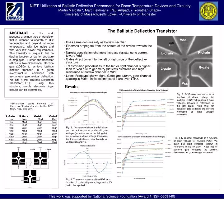
NIRT: Utilization of Ballistic Deflection Phenomena for Room Temperature Devices and Circuitry Martin Margala *, Marc Feldman+, Paul Ampadu+, Yonathan Shapir+ *University of Massachusetts Lowell, +University of Rochester. The Ballistic Deflection Transistor.

E N D
NIRT: Utilization of Ballistic Deflection Phenomena for Room Temperature Devices and Circuitry Martin Margala *, Marc Feldman+, Paul Ampadu+, Yonathan Shapir+ *University of Massachusetts Lowell, +University of Rochester The Ballistic Deflection Transistor ABSTRACT - This work presents a unique type of transistor that is intended to operate to THz frequencies and beyond, at room temperature, with low noise and with very low power requirements. This transistor is unique in that no doping junction or barrier structure is employed. Rather, the transistor utilizes a two-dimensional electron gas (2DEG) to achieve ballistic electron transport in a gated microstructure, combined with asymmetric geometrical deflection. We call it the "Ballistic Deflection Transistor"(BDT). Using this structure, simple electronic logic circuits can be assembled. Vdd • Uses same non-linearity as ballistic rectifier • Electrons propagate from the bottom of the device towards the top • Narrow constriction channels increase resistance to current toward Vdd • Gates direct current to the left or right side of the deflective structure • Transmission probabilities to the left or right channel is higher than to Vdd due to geometry (deflects electrons and high resistance of narrow channel to Vdd) • Latest Prototype shown right. Gates are 430nm, gate-channel spacing is 80nm. Initial estimates of ft are over 1THz. R-drain L-drain R-gate L-gate Vss Results Fig. 3. IV Current responds as a function of drain voltage for multiple NEGATIVE push pull gate voltages (shown in reference to the left gate). Note that for negative gate voltages the current increases as gate voltage increases. • Simulation results indicate that there are 3 natural states to the BDT: High, Med, and Low. L Gate R Gate Out-L Out–R Low Low Med Med Low Med High Low Low High High Low Med Low Low High Med Med Med Med Med High High Low High Low Low High High Med Low High High High Med Med Fig. 2. IV characteristic of the left drain port as a function of push-pull gate voltage (in reference to the left gate), an increase in drain voltage increases the transconductance, near linearly for voltage beyond 1V. Fig. 4. IV Current responds as a function of drain voltage for multiple POSITIVE push pull gate voltages (shown in reference to the left gate). Note that for positive gate voltages the current decreases as gate voltage increases. Fig. 5. Transconductance of the BDT as a function of push-pull gate voltage with a 2V drain bias applied. This work was supported by National Science Foundation (Award # NSF-0609140)