Download
1 / 4
40 likes | 288 Views
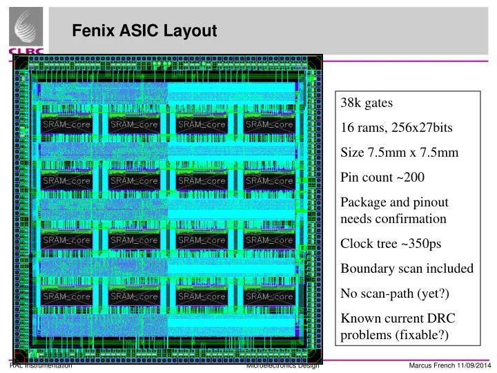
Fenix ASIC Layout. 38k gates 16 rams, 256x27bits Size 7.5mm x 7.5mm Pin count ~200 Package and pinout needs confirmation Clock tree ~350ps Boundary scan included No scan-path (yet?) Known current DRC problems (fixable?). Fenix Layout Detail. Fenix Synthesis and Place and Route Flow.

E N D
Fenix ASIC Layout 38k gates 16 rams, 256x27bits Size 7.5mm x 7.5mm Pin count ~200 Package and pinout needs confirmation Clock tree ~350ps Boundary scan included No scan-path (yet?) Known current DRC problems (fixable?)
Fenix Synthesis and Place and Route Flow Other issues: LVS and DRC steps SRAM testing Embedded self-test
Fenix Simulation and Conformity Check Other issues: Test vector generation Packaging Bonding diagram Test strategy (both packaged and PCB)