Download
1 / 29
290 likes | 355 Views
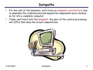
We’ll focus on computer architecture : how to assemble the combinational and sequential components we’ve studied so far into a complete computer. The datapath is the part of the central processing unit (CPU) that does the actual computations. Chapter 10-Datapaths.

E N D
We’ll focus on computer architecture: how to assemble the combinational and sequential components we’ve studied so far into a complete computer. The datapath is the part of the central processing unit (CPU) that does the actual computations. Chapter 10-Datapaths
Abstraction is very helpful in understanding processors. Although we studied how devices like registers and muxes are built, we don’t need that level of detail here. You should focus more on what these component devices are doing, and less on how they work. Otherwise, it’s easy to get bogged down in the details, and datapath and control units can be a little intimidating. Keeping it simple!
We can divide the design of our CPU into three parts: The datapath does all of the actual data processing. An instruction set is the programmer’s interface to CPU. A control unit uses the programmer’s instructions to tell the datapath what to do. We’ll look in detail at a processor’s datapath, which is responsible for doing all of the dirty work. An ALU does computations, as we’ve seen before. A limited set of registers serve as fast temporary storage. A larger, but slower, random-access memory is also available. An overview of CPU design
A processor is just one big sequential circuit. Some registers are used to store values, which form the state. An ALU performs various operations on the data stored in the registers. ALU Registers What’s in a CPU?
Fundamentally, the processor is just moving data between registers, possibly with some ALU computations. To describe this data movement more precisely, we’ll use a register transfer language. The objects in the language are registers. The basic operations are transfers, where data is copied from one register to another. We can also use the ALU to perform arithmetic operations on the data while we’re transferring it. ALU Registers Register transfers
Two-character names denote registers, such as R0, R1, DR, or SA. Arrows indicate data transfers. To copy the contents of the sourceregister R2 into the destinationregister R1 in one clock cycle: R1 R2 A conditional transfer is performed only if the Boolean condition in front of the colon is true. To transfer R3 to R2 when K = 1: K: R2 R3 Multiple transfers on the same clock cycle are separated by commas. R1 R2, K: R2 R3 Don’t confuse this register transfer language with assembly language, which we’ll discuss later. Register transfer language review (from Chapter 7)
We can apply arithmetic operations to registers. R1 R2 + R3 R3 R1 - 1 Logical operations are applied bitwise. AND and OR are denoted with special symbols, to prevent confusion with arithmetic operations. R2 R1 R2 bitwise AND R3 R0 R1 bitwise OR Lastly, we can shift registers. Here, the source register R1 is not modified, and we assume that the shift input is just 0. R2 sl R1 left shift R2 sr R1 right shift Register transfer operations (cont’d)
We’ll use this block diagram to represent an n-bit register. There is a data input and a load input. When Load = 1, the data input is stored into the register. When Load = 0, the register will keep its current value. The register’s contents are always available on the output lines, regardless of the Load input. The clock signal is not shown because it would make the diagram messy. Remember that the input and output lines are actually n bits wide! Load Data input R0 n n Data output Block symbols for registers
Modern processors have a number of registers grouped together in a register file. Much like words stored in a RAM, individual registers are identified by an address. Here is a block symbol for a 2k x n register file. There are 2k registers, so register addresses are k bits long. Each register holds an n-bit word, so the data inputs and outputs are n bits wide. D n D data WR Write k DA D address Register File k k AA A address B address BA A data B data n n A B Register file
You can read two registers at once by supplying the AA and BA inputs. The data appears on the A and B outputs. You can write to a register by using the DA and D inputs, and setting WR = 1. These are registers so there must be a clock signal, even though we usually don’t show it in diagrams. We can read from the register file at any time. Data is written only on the positive edge of the clock. Accessing the register file D n D data WR Write k DA D address Register File k k AA A address B address BA A data B data n n A B
Here’s a 4 x n register file. (We’ll assume a 4 x n register file for all our examples.) n n n What’s inside the register file
The 2-to-4 decoder selects one of the four registers for writing. If WR = 1, the decoder will be enabled and one of the Load signals will be active. The n-bit 4-to-1 muxes select the two register file outputs A and B, based on the inputs AA and BA. We need to be able to read two registers at once because most arithmetic operations require two operands. Explaining the register file
The main job of a central processing unit is to “process,” or to perform computations....remember the ALU from way back when? We’ll use the following general block symbol for the ALU. A and B are two n-bit numeric inputs. FS is an m-bit function select code, which picks one of 2m functions. The n-bit result is called F. Several status bits provide more information about the output F: V= 1 in case of signed overflow. C is the carry out. N= 1 if the result is negative. Z= 1 if the result is 0. m n n n A B FS ALU V C N Z F The all-important ALU
For concrete examples, we’ll use the ALU as it’s presented in the textbook. The table of operations on the right is taken from the book. The function select code FS is 5 bits long, but there are only 15 different functions here. We use an alternative notation for AND and OR to avoid confusion with arithmetic operations. ALU functions
Here is the most basic datapath. The ALU’s two data inputs come from the register file. The ALU computes a result, which is saved back to the registers. WR, DA, AA, BA and FS are control signals. Their values determine the exact actions taken by the datapath— which registers are used and for what operation. Remember that many of the signals here are actually multi-bit values. D data WR Write DA D address Register File 5 2 2 2 AA A address B address BA A data B data A B FS FS ALU V n n n C N Z F Our first datapath
Let’s look at the proper control signals for the operation below: R0 R1 + R3 Set AA=01 and BA=11. This causes the contents of R1 to appear at A data, and the contents of R3 to appear at B data. Set the ALU’s function select input FS = 00010 (A + B). Set DA = 00 and WR = 1. On the next positive clock edge, the ALU result (R1 + R3) will be stored in R0. An example computation D data WR Write 1 DA D address 00 Register File AA BA A address B address 01 11 A data B data A B FS FS 00010 ALU V C N Z F
Four registers isn’t a lot. What if we need more storage? Who exactly decides which registers are read and written and which ALU function is executed? D data WR Write DA D address Register File AA A address B address BA A data B data A B FS FS ALU V C N Z F Two questions
Here’s a way to connect RAM into our existing datapath. To write to RAM, we must give an address and a data value. These will come from the registers. We connect A data to the memory’s ADRS input, and B data to the memory’s DATA input. Set MW= 1 to write to the RAM. (It’s called MW to distinguish it from the WR write signal on the register file.) RAM n ADRS n n n DATA OUT +5V CS MW WR n D0 Q D1 S We can access RAM also D data WR Write DA D address Register File AA A address B address BA A data B data A B FS FS 1 V ALU C N Z F MD
To read from RAM, A data must supply the address. Set MW = 0 for reading. The incoming data will be sent to the register file for storage. This means that the register file’s D data input could come from either the ALU output or the RAM. A mux MD selects the source for the register file. When MD = 0, the ALU output can be stored in the register file. When MD = 1, the RAM output is sent to the register file instead. n n n D0 Q D1 S Reading from RAM n D data WR Write DA D address Register File AA A address B address BA A data B data RAM n ADRS DATA OUT +5V CS A B MW WR FS FS 0 V ALU C N Z F MD
We now have a way to copy data between our register file and the RAM. Notice that there’s no way for the ALU to directly access the memory—RAM contents must go through the register file first. Here the size of the memory is limited by the size of the registers; with n-bit registers, we can only use a 2n x n RAM. For simplicity we’ll assume the RAM is at least as fast as the CPU clock. (This is definitely not the case in real processors these days.) D data WR Write DA D address Register File AA A address B address BA A data B data RAM ADRS n n n n DATA OUT +5V CS A B MW WR FS FS V ALU C N Z F n D0 Q D1 S MD Notes about this setup
In our transfer language, the contents at random access memory address X are denoted M[X]. For example: The first word in RAM is M[0]. If register R1 contains an address, then M[R1] are the contents of that address. The M[ ] notation is like a pointer dereference operation in C or C++. Memory transfer notation
Here is a simple series of register transfer instructions: R3 M[R0] R3 R3 + 1 M[R0] R3 This just increments the contents at address R0 in RAM. Again, our ALU only operates on registers, so the RAM contents must first be loaded into a register, and then saved back to RAM. R0 is the first register in our register file. We’ll assume it contains a valid memory address. How would these instructions execute in our datapath? Example sequence of operations
AA should be set to 00, to read register R0. The value in R0 will be sent to the RAM address input, so M[R0] appears as the RAM output OUT. MD must be 1, so the RAM output goes to the register file. To store something into R3, we’ll need to set DA = 11 and WR = 1. MW should be 0, so nothing is accidentally changed in RAM. Here, we did not use the ALU (FS) or the second register file output (BA). n n D0 Q D1 S R3 M[R0] n 1 D data WR Write DA D address 11 Register File AA A address B address BA 00 A data B data RAM n ADRS DATA OUT +5V CS A B MW WR FS FS 0 V ALU C N Z F n MD 1
AA = 11, so R3 is read from the register file and sent to the ALU’s A input. FS needs to be 00001 for the operation A + 1. Then, R3 + 1 appears as the ALU output F. If MD is set to 0, this output will go back to the register file. To write to R3, we need to make DA = 11 and WR = 1. Again, MW should be 0 so the RAM isn’t inadvertently changed. We didn’t use BA. n n n R3 R3 + 1 n 1 D data WR Write DA D address 11 Register File AA A address B address BA 11 A data B data RAM ADRS DATA OUT +5V CS 00001 A B MW WR FS FS 0 V ALU C N Z F n D0 Q D1 S MD 0
Finally, we want to store the contents of R3 into RAM address R0. Remember the RAM address comes from “A data,” and the contents come from “B data.” So we have to set AA = 00 and BA = 11. This sends R0 to ADRS, and R3 to DATA. MW must be 1 to write to memory. No register updates are needed, so WR should be 0, and MD and DA are unused. We also didn’t use the ALU, so FS was ignored. n n n D0 Q D1 S M[R0] R3 0 D data WR Write DA D address Register File AA A address B address BA 00 11 A data B data RAM n ADRS n DATA OUT +5V CS A B MW WR FS FS 1 V ALU C N Z F MD
One last refinement is the addition of a Constant input. The modified datapath is shown on the right, with one extra control signal MB. We’ll see how this is used later. Intuitively, it provides an easy way to initialize a register or memory location with some arbitrary number. D data WR Write DA D address Register File AA A address B address BA A data B data RAM ADRS DATA OUT +5V CS MW WR A B FS FS V ALU C N Z D0 F Q D1 S Constant in Constant MB S D1 D0 Q MD
From these examples, you can see that different actions are performed when we provide different inputs for the datapath control signals. The second question we had was “Who exactly decides which registers are read and written and which ALU function is executed?” In real computers, the datapath actions are determined by the program that’s loaded and running. A control unit is responsible for generating the correct control signals for a datapath, based on the program code. We’ll talk about programs and control units later. Control units
The datapath is the part of a processor where computation is done. The basic components are an ALU, a register file and some RAM. The ALU does all of the computations, while the register file and RAM provide storage for the ALU’s operands and results. Various control signals in the datapath govern its behavior. Next, we’ll see how programmers can give commands to the processor, and how those commands are translated in control signals for the datapath. Summary
HW 10 1. Design a 4 bit arithmetic circuit, with two selection variables S1 and S0, that generates the arithmetic operations below. Draw the logic diagram for a single bit stage. (Q 10-4) 2. A computer has a 32 bit instruction word broken into fields as follows: opcode, 6 bits; two register fields, 6 bits each; and one immediate operand/register field, 14 bits. • (a) What is the maximum number of operations that can be specified? • (b) How many registers can be addressed? • (c) What is the range of unsigned immediate operands that can be provided? (Q 10-13)