Download
1 / 22
230 likes | 407 Views
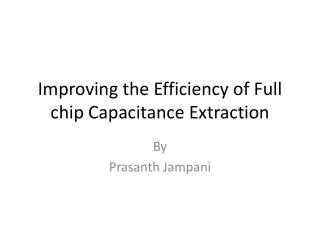
Improving the Efficiency of Full chip Capacitance Extraction. By Prasanth Jampani. Capacitance of an interconnect. Capacitance of a segment of a net can be divided into three components : area Ca, fringe Cf and lateral Cl

E N D
Improving the Efficiency of Full chip Capacitance Extraction By Prasanth Jampani
Capacitance of an interconnect • Capacitance of a segment of a net can be divided into three components: area Ca, fringe Cf and lateral Cl • Ca: overlap capacitance due to the overlap of two conductors in different layers • Cl: Lateral capacitance between two conductors in the same plane • Cf: Fringe coupling capacitance between two conductors in different planes • Full Chip Capacitance Extraction • Plays a very important role in determining circuit performance for very deep sub-micron technology. • As the interconnect density and the operational frequency in a chip increase, the extraction of interconnect parasitics becomes more and more time consuming. • This is particularly true if one were to target the extraction of 3-D (three-dimensional) parasitics.
Rule Based Approach • get the area overlap, multiply by the corresponding area coefficient • get the edge length, multiply by the corresponding edge coefficient • The coefficient is obtained by using a 3D field solver on each configuration that is identified. • Ignore the lateral capacitance (Major Limitation) • This approach is being used in P&R, Floor planning tools as this is very simple and quick Different fringe capacitance coef for different layer combinations Lateral capacitance coefficient is difficult
Formula based approach • This approach separates the three capacitance effects and uses a separate formulation for each of the effects. • Where C0,C1,C2,C3 and C4 are constants arrived at after fitting this equation to the 2D-simulated lateral capacitance data.
Formula based approach(Cont..) • There will be a separate set of constants for each vertical profile and will be retrieved through table look-up. • This approach uses a combination of equation calculation with table look-up • Considered to have 2 1/2D accuracy
Table Based Approach • A typical library for a process with 3 layers of metal contains tens of thousands of entries. • The interconnect is decomposed into the primitives to match with the patterns in the library. • A 3D field solver is called for non-matched patterns. Field Solvers • Several field solvers are available in the market • finite difference method: Raphael from TMA • finite element method: Maxwell from Ansoft, Metal from OEA International • boundary element method: Arcadia from Synopsys, Fastcap • Field solvers are mainly used to characterize the library • Due to the slow speed, it is not practical to use field solvers to perform full chip extraction. • Field solver can be combined with table approach to provide acceptable performance.
Full Chip extraction techniques • Quasi-3D with table lookup • Calculate several cross sections capacitance(using 2D method) and combine the 2D results into the 3D capacitance value. • As 2D field solver is much faster than 3D, it greatly improves the efficiency of capacitance extraction. • Loss of accuracy (error up to 10%). • “2X2D”, ‘3X2D”. • computation speed is still not satisfactory for full chip extraction for large layout with multi-million gates. • A natural idea to speedup is to build a library storing the capacitance values for most regular patterns. When these patterns are met during extraction, just lookup and get the capacitance value. • Compared with 3D field solver, quasi-3D method greatly improves computational speed.
Quasi-3D with table lookup (cont..) • The capacitance on the cross section of YOZ and XOZ is calculated by 2D field solver. • Total 3D capacitance can be given by C = Cyoz * L + Cxoy * H + Cxoz * W, where Cyoz, Cxoy and Cxoz are calculated using 2D field solver(BEM).
Quasi-3D with table lookup (cont..) • There are large areas on conductor surfaces which could not be counted to 3D capacitance if only using 2D orthogonal cross sections. • To generate the model library we choose design parameters(metal width, metal spacing etc as variables and technology parameters set to constant in the capacitance expression • In the process of full chip extraction, every time it meets a 2D shaper, the program automatically search the library to find the pattern. • If found, used the equation, otherwise use the 2D field solver.
Extraction using vertical profile • Uses vertical profile( The sequence of material layers that are present in vertical dimension at any point). • The layout geometry is divided into vertical stripes and each stripe is processed independently. • Each stripe is fractured into elemental areas that consist of rectangles. Each elemental area has a unique vertical profile. • Capacitance for each elemental area is done based on the models and their coefficients stored in the library for different profiles. • The elemental areas associated with a given node are then summed to give the total lumped capacitance for each node. • Model library for all the vertical profiles has to be generated. Top view Side view showing 4 vertical profiles Different vertical profiles in a more complex 3D structure
Accuracy Comparison • There are many claims to accuracy based on the approach, Quasi-3D, 3D-like, true 3D, etc • All implementations contain a trade-off of accuracy for higher • performance. • Accuracy comparison should be based on real patterns coming from actual design. The patterns should not include those used in characterizing the library. • The average difference from 3D field solver is a good measure. 3D Effects • Some 3D fields are not included in the equation or Quasi-3D approach
Idea of new approach • By using Quasi-3D and Vertical profiling methods we get only 2D accuracy. • We may require 3D efficiency at some nodes in the circuit. • In the new extraction algorithm, we try to take into account both the 2D and 3D field solver to improve the accuracy and at the same time not sacrificing much on the time constraint. • This is coupled with the pattern matching from a model library. • The model library maintains most of the common 2D patterns and at the same time some critical 3D models(should decide on what are critical???). • Pattern matching is an important part of the algorithm. • In this approach, extract different patterns from the top view of the circuit instead of taking cross sections to support the selection of different field solvers and to cover more number of patterns. • We are planning to use OpenAccess (www.si2.org) database as a base for the application. • The next few slides talk about the pattern extraction, which is an important part of the capacitance extraction .
Pattern Extraction Algorithm Step 1: Extract the interconnect information from the layout file (GDS2 or LEF/DEF) Step 2: Find out different horizontal and vertical interconnections of different metal layers (considering only Manhattan geometry). Step 3: Divide the entire chip area into several rectangular blocks (rows and columns) . Minimum block size is maintained to get proper affect of neighboring conductors on a target. Step 4: Find out the pattern in each block • If it is the basic pattern and matching with the one in the model library, then goto step 5. • Stop sub-dividing even though there is no pattern in the model library if the complexity (which can be decided by the number of horizontal and vertical lines) is less than some threshold. • With 2D/3D field solver, calculate the capacitance data for this patter and update the model library. • Otherwise (if the complexity is more than the threshold), subdivide the block into several smaller blocks and repeat step 4 Step 5: Get the predefined capacitance coefficients from the library and extract the capacitance value. Notes: • The initial size of the block depends on the complexity of the chip layout. The best value can be found with experimentation. • If a specific block contains more complex structures, then divide it into sub blocks to reduce the complexity.
Example Blocks Bounding Box (Chip Area) Find out the patterns in each Block. It the block is more complex, Divide into sub blocks Metal 1 Metal 2 Metal 3
Implementation Intermediate file with the required information to extract different patterns Extracts the Interconnect NETs information Perl Script Pattern Extraction Algorithm Interconnects File DEF File patterns Pattern matching OpenGL Rendering Engine 2D/3D Model Library spice Circuit Netlist Screen
Results(sample run) • Input DEF File: c17.def • Interconnects file: c17.txt Perl script • C17.txt is given as input to the pattern Extraction algorithm • User input to the Algorithm: • Total number of blocks (No of Rows * No of Columns) • The complexity of the pattern -> Maximum number of horizontal and vertical lines allowed in the pattern. This value can be the sum of total lines. • Total area is divide into 5X5 = 25 blocks
Future Work • Improve the efficiency of the pattern matching algorithm and compare the results with the commercial tools like Hicap. • Development of full chip extraction tool on OpenAccess Database Stream to OpenAccess Mapping Pattern Extraction Algorithm GDS2 2D/3D Model Library Capacitance Models 2D/3D numerical simulations Capacitance Data Capacitance Extraction OpenAccess Database
OpenAccess • A Common design database – OA DB (publicly available). No need of individual databases. • Provides an interoperability platform for complex IC design based on a common, open, and extensible architecture. • This is achieved through an open standard application programming interface (API) and reference database implementation supporting that API. • Common method to represent the elements of IC design data and a common API to access and manipulate that data. • OA makes extensive use of IC-specific data compression techniques to reduce the memory footprint, to address the size, capacity, and performance problems of previous DBs. • A logically central repository for design information makes it possible to overcome key failings of traditional EDA environnent. • A common information model enables great efficiencies by eliminating data translation among design and analysis tools. • Integrators of Computer-Aided Design (CAD) systems for ICs and application developers can focus on methodology and functionality rather than the incompatibilities in communication between design tools. • Translators are useful for validating the migration of applications to the OpenAccess DB. • Interoperability among the ID design tools.