Download
1 / 7
70 likes | 194 Views
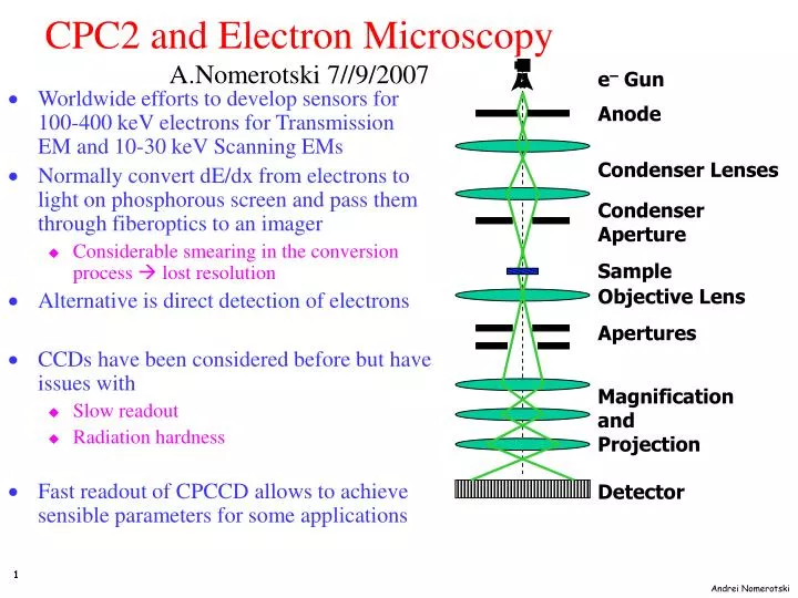
e – Gun. Anode. Condenser Lenses. Condenser Aperture. Sample. Objective Lens. Apertures. Magnification and Projection. Detector. CPC2 and Electron Microscopy A.Nomerotski 7//9/2007.

E N D
e– Gun Anode Condenser Lenses Condenser Aperture Sample Objective Lens Apertures Magnification and Projection Detector CPC2 and Electron Microscopy A.Nomerotski 7//9/2007 • Worldwide efforts to develop sensors for 100-400 keV electrons for Transmission EM and 10-30 keV Scanning EMs • Normally convert dE/dx from electrons to light on phosphorous screen and pass them through fiberoptics to an imager • Considerable smearing in the conversion process lost resolution • Alternative is direct detection of electrons • CCDs have been considered before but have issues with • Slow readout • Radiation hardness • Fast readout of CPCCD allows to achieve sensible parameters for some applications
Beam entrance Enclosure Vacuum tight connectors CPC2 in MB4 Oxford Materials • Oxford Materials (Angus Kirkland, Grigore Moldovan et al) are interested to use CPC2 to study effects of multiple- and back- scattering of 200 keV electrons in silicon • The Group has several TEM and SEM both in Oxford and Begbroke • Discussions started last autumn, during spring-summer 2007 prepared vacuum enclosure and cabling to accommodate MB4 with SLM CPC2-10 under the microscope
CPC2 in Vacuum Enclosure • All assembled and tested in vacuum • Noise 80 e with final cabling in the lab, about 100 e at Begbroke • Data taking 29-30August • Team : G.Moldovan, Ron (TEM tech), P.Coulter, B.Jeffery, AN • Simple DAQ and monitoring by Ben • Took a day to get acceptable vacuum at microscope, a lot of outgassing • Immediately saw clusters from 200 keV e • Took ~20 runs at various conditions: intensity, energy (80-200 keV), sensor temperature, integration time, clock frequency • Ran at +45 deg C (one run at +30 deg C) so had to trigger as fast as possible, otherwise leakage current saturate the well • Took data at 1, 2 and 5 ms integration times
Simulated Tracks 100 keV e– • By P.Denes at STD06 • To have best resolution the sensor should be as thin as possible – requirement similar to ILC • Backscattering is a considerable effect 100 m Si 300 keV e SiO2 + metal Si epi 300 keV e– 300 m Si 40 µm
Simulation of Clusters Charge/pixel in electrons • Grigore simulated 20x20x25 micron pixels at different e energies: 100, 200, 300 and 400 keV • At 200 keV • charge/pixel peaks at 2500 e • Peak in charge distribution scales as 1/b2 • Equally probable to have one and two pixel clusters Cluster size
Status & Plans • Data analysis • Converted ADC data to 4x700 pixel images in LabVIEW (Ben) • 16 14-bit ADC words one 16-bit word after CDS (.png format) • Use ImageJ freeware for cluster analysis, this is routinely used by Materials for image analyses (Grigore, Philip) • First plots to produce: total charge, cluster size, cluster shape (orientation, sphericity), distance to closest neighbour, correlation between variables • Issues we know of: Charge spilling between pixels • Well capacity is only ~8 ke and it’s partly filled in by dark current • Good: charge is not lost • Bad: cluster shape can be distorted • Handles to study: vertical and horizontal spilling are different • Plan another run in a couple of weeks to take a knife blade image • For imaging need integration time to be (much) longer than readout time • Plan to install a Peltier near CPC2 to cool it decrease dark current • Mid term – compare to simulation and write a paper, it looks like this could be the first ever direct detection data taken with fine pitch silicon pixel detector at TEM