Download
1 / 25
250 likes | 350 Views
SVX4 Silicon Readout Chip for Fermilab. R. J. Yarema June 9, 2003. Generations of SVX Silicon Strip Readout Chips. SVX 1986-89 UTMC 3.0 µ 128 3 µsec None Analog No No 6.3x4.6 ? Mrad CDF. SVX2 1993-96 UTMC 1.2 µ 128 132/396 ns 32 cells 8 bit Yes No 6.3x8.9 10 Mrad DO.

E N D
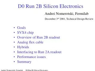
SVX4 Silicon Readout Chip for Fermilab R. J. Yarema June 9, 2003
Generations of SVX Silicon Strip Readout Chips SVX 1986-89 UTMC 3.0 µ 128 3 µsec None Analog No No 6.3x4.6 ? Mrad CDF SVX2 1993-96 UTMC 1.2µ 128 132/396 ns 32 cells 8 bit Yes No 6.3x8.9 10 Mrad DO SVX3 1995-98 Honeywell 0.8µ 128 132/396 ns 42 cells 8 bit Yes Yes 6.3x11.9 10 Mrad CDF SVX4 2000-03 TSMC 0.25µ 128 132/396 ns 42 cells 8 bit Yes Yes 6.3x9.0 50 Mrad min CDF/DO Development Foundry Feature size Channels Beam Crossing Storage Signal output Programmable Deadtimeless Chip Size (mm) Radiation Experiment Phenix Collaboration Meeting
96 m Diced width ~ 6.40mm Channel 127 Channel 0 SVX4 Chip Detector pitch = 50µ Diced length ~ 9.11 mm Electronics channel pitch = 42 µ Active area = 57 mm2 Phenix Collaboration Meeting
SVX4 Features • 128 channels per chip • Maximum interaction rate equal to 132 nsecs • Optimized for capacitive loads from 10-35 pF • Channel mask with dual functionality: used for either charge injection or masking channels with excessive DC current from the detector • Choice of operation in either D0 or CDF mode using an external pad as selector • Selectable input bandwidth • Double correlated sampling (see section 2.2.1) • Large dynamic range on input integrator to minimize dead time due to pre-amplifier resets • Programmable analog pipeline (47 cells, 42 cells maximum depth for pipeline, 4 cells for trigger buffer, 1 cell for write amplifier pedestal) • Digitization of analog signals with up to 8 bits of resolution using a modified Wilkinson type ADC • Dynamic pedestal subtraction Phenix Collaboration Meeting
Features (Continued) 12. Data sparsification (zero suppression) 13. Neighbor channel readout selection (cluster readout) 14. Low noise (S/N=10:1 to 20:1 for input capacitances from 35 pF to 10 pF for an input charge equivalent to 1 MIP = 4 fC) 15. Low power consumption (approximately 3 mW/channel) to minimize the cooling requirements 16. Operation with a single voltage source (even though two separate decoupled supplies for the analog and the digital portions of the chip may be required). 17. Operation compatible with single-sided AC coupled silicon strip detectors 18. Ability to inject charge for testing and calibration in each channel 19. Daisy chain operation capability 20. Parallel bus data readout 21. Integral Data Valid strobe signal in the data bus (OBDV) 22. Can be implemented in the TSMC (Taiwan Semiconductor Manufacturing Company) 0.25 micron process, which is inherently a radiation hard process Phenix Collaboration Meeting
Operating Modes • Initialize • Acquire • Digitize • Readout For deadtimeless operation, the chip is first initialized, then acquire takes place continuously and the chip switches between digitize and readout. Phenix Collaboration Meeting
Initialization bit stream (192 bits) • 0:127 cal mask or channel disable • 128 spare • 129 connects Vcal • 130 selects cal mask or disable register for bits 0:127 • 131:134 preamp risetime • 135:138 preamp input FET bias • 139:140 pipeline write amp bias • 141:142 pipeline read amp bias • 143:148 clock ticks to level one accept • 149 pipeline readout order • 150:156 Chip ID • 157 disable pedestal substraction • 158 always read channel 128 Phenix Collaboration Meeting
Initialization bits (continued) • 159 Always read channel 63 • 160:161 readout hit, or hit + neighbors, or all channels • 162:165 ADC ramp pedestal • 166 ADC ramp direction • 167 ADC ramp direction • 168:170 ADC ramp range • 171:178 ADC digital threshold • 179:186 ADC counter modulo • 187 first chip in daisy chain flag • 188 last chip in daisy chain flag • 189:191 output driver current Phenix Collaboration Meeting
Reset ~ 4 fC/MIP ~5mv/fC = 20 mV/MIP n p Ccoupling - Rbias SVX4 Input Amplifier/Integrator + Si Strip Detector (300 m thick) Preamp operation Phenix Collaboration Meeting
Pipeline and ADC Operation Phenix Collaboration Meeting
Byte no Content Comments 1 Chip ID Has highest bit set to 1, the rest are derived from the downloaded parameters (i.e. lowest value in Hex is “80”) 2 Pipeline Cell Number True (physical) number of cell being digitized Can be 1 to 42 decimal (but not 0), the two most significant bits are always 0. 3 Channel ID Can be 0 to FE hex (127 decimal), increasing. 4 Data for above Channel ID Gray Coded (0 to 255 decimal) … … Last-1 Channel ID Can be 0 to FE hex (127 decimal), increasing. Last Data for Above Channel ID Gray Coded (0 to 255 decimal) Output Data Stream Format Phenix Collaboration Meeting
Chip Readout The minimal readout is 2 bytes (Chip ID and Pipeline Cell) and no data, due to no channel being above pedestal, and also Read All, Read 127, and Read 63 bits being off . Phenix Collaboration Meeting
Performance • Input noise is 400 + 42 erms/pf @ 132 ns • Gain is 15 mv/fC • Input dynamic range is about 200 fC • Pipeline dynamic range is about 60 fC • Acquisition clock runs at 2.5 to 7.5 Mhz • Analog current = 50 ma, digital current = 20 ma • Power = 175 mw/chip • Readout clock run at 53 Mhz • Digitization at 53 Mhz • Readout at 106 Mhz (both edges of readout clock) Phenix Collaboration Meeting
0.25 µm TSMC Wafer Yield • Engineering run (1 lot, 12 wafers) – 100% • SVX4 (version 1 and 2) and TRIP • Engineering run (2 lots, 24 wafers) – 91% • TXM25 and FPIX2 • Engineering run (1 lot, 25 wafers) – 96% • One wafer dropped and broken • SVX4 only (versions A and B) Average is better than 95% Phenix Collaboration Meeting
SVX4_V1 and V2 wafer probing • 12 wafers total, 9 with probing results • (2 diced before tests, 1 with some suspect results) • 9 wafers probed for current measurements • 18/936 chips fail with bad current draw on either AVDD or DVDD (i.e. shorts) (1.9%) • ~7 wafers probed for basic functionality • 37/762 chips have a small problem (bad channel(s), fail sparsification, etc.) (4.3%) • 3 V2 wafers tested fully (all pipeline cells etc.) • 4/156 chips have a very small problem (more than one bad pipeline cell, noisy, etc.) (2.6%) • Overall yield: 91.2% perfect, 97% functional ! Phenix Collaboration Meeting
SVX4_2a and _2b wafer probing • 11/11 initial devices looked good (basic functionality) – before grinding and plating • 56 devices looked at after grind/plating • 2 bad (current draws) • 10 with one or two bad channels • 4 with higher pedestal (needs investigation) • Note: many of the 56 devices were close to the wafer’s edge • No yield estimate until several 100’s are probed. Phenix Collaboration Meeting
Automated Wafer Testing for Known Good Die Phenix Collaboration Meeting
Major improvement in 2nd Run • Much more uniform channel to channel pedestal across the chip. Phenix Collaboration Meeting
Extreme settings to highlight the bow: Minimize time between Comp and ramp resets Ramp Ped set to max (lowest pedestal) or 9 for _V2 and 10 for _2x DVDD = 2.75 V (AVDD = 2.5 V) Offset of 15 cnts between _2a and_2b exists for other ramp ped settings. Versions 1 and 2 Version B Version A Phenix Collaboration Meeting
Pedestal Uniformity Between Cells in a Channel Pedestal vs pipeline cell for a single channel during various operations. SVX4_V2 (older version) compared with SVX4_2b (newer version). small slope over 46 pipeline cells is observed. Small coupling of chip operation into pedestal readout. Version 1 and 2 Versions A and B Phenix Collaboration Meeting
SVX4 Cost • Fabrication through MOSIS • $5000/wafer (no overhead included) • 312 die/wafer • Assuming 75% yield, cost = $21/chip • Cost might be cheaper going through Fermi/Taiwan collaboration. Overhead charges? • Could be asked to contribute to development cost of SVX4. Phenix Collaboration Meeting
Other related developments • TRIP chip for VLPCs and scintillating fibers • 32 channels with preamp and disc • Used SVX4 pipeline, added mux for analog output. Used portion of FPIX slow control. • 4.8 x 4.55 mm. • Designed for 30-40 pf, fast risetime (tr=12 ns) • Reset every BCO • ENC = 2400 erms @ C=0 pf • Engineering design time = 6 man-months + testing • Built production quantity (6864) with no prototypes Phenix Collaboration Meeting
TRIP Chip SVX4 pipeline Adapted from FPIX slow control Phenix Collaboration Meeting
Other related developments (cont.) • FSSR – silicon strip readout for BTEV • Design in progress • 128 channels with binary readout • New preamp and discriminator, no pipeline • Programmable serial interface and readout based on FPIX design • 7.5 mm x 4.5 mm (34 mm2) on 50 u pitch • ENC = 300 erms @ 0 pf and tr = 85 ns. • Engineering design time = 6-8 man-months for first submission • Full size chip submission expected July ‘03 Phenix Collaboration Meeting
Conclusion • SVX4 is ready for production. • Many silicon strip and similar readout devices have been designed. • Full custom design of some chips can be relatively fast, especially when using ideas developed in previous designs. Phenix Collaboration Meeting